Hello!
In our last lesson, we focused on quantifying hard-switching losses, calculating the power dissipated due to the simultaneous overlap of voltage and current. We established that these losses are a major source of inefficiency, especially as switching frequencies increase.
Today, we'll investigate the other major drawback of hard switching: the generation of electromagnetic interference (EMI). Your learning goal for this lesson is to describe the sources and impacts of EMI in hard-switched converters. This is the final piece of the "hard switching problem" puzzle. Understanding where this electrical noise comes from and why it's a problem is essential for reviewing and optimizing real-world circuits, and it will highlight another powerful benefit of the ZVS techniques we'll be exploring soon.
The Root Cause: Fast Edges, Wide Noise
In the previous lessons, we identified the rapid transitions of voltage and current (high and ) as the cause of switching loss. These same fast edges are also the fundamental source of EMI.
From a signal processing perspective, which might be familiar from your CS background, a sharp edge in the time domain (like a square wave) is composed of a fundamental frequency plus a very wide spectrum of higher-frequency harmonics. The faster the edge, the more energy is contained in those high-frequency harmonics. This is not just a theoretical concept; it has very real consequences in power electronics.
This video demonstrates exactly how slowing down a MOSFET's switching speed affects the noise spectrum.
Impact of MOSFET Gate Resistor on the EMI & Noise Spectrum of a Switch Mode Power Supply
The video 'Impact of MOSFET Gate Resistor on the EMI & Noise Spectrum' by Biricha Digital provides a clear, practical link between switching speed and generated noise.
Please watch the following two segments: Theoretical Explanation (0:45 - 4:06): Focus on the core concept: faster rise times (TR) lead to more high-frequency harmonic content. Lab Demonstration (5:30 - 7:47): Observe how changing the gate resistor from 0 ohms (very fast switching) to 100 ohms (slow switching) dramatically reduces the noise measured on the spectrum analyzer. This directly visualizes the theory.
As the video shows, there is a direct trade-off: fast switching is good for reducing the duration of the V-I overlap (improving efficiency), but it generates more high-frequency noise. This noise is the "E" in EMI.
A Framework for Understanding EMI: Source, Path, Victim
All EMI problems can be broken down into three components:
- Source: The origin of the noise. In our case, it's the fast-switching MOSFET.
- Coupling Path: The route the noise takes to get from the source to where it can cause problems.
- Victim (or Receiver): A circuit or component that is adversely affected by the noise. This could be the power supply's own control logic, nearby electronics, or the test equipment used for regulatory certification.
Our focus today is on the sources and the coupling paths, as these are what we can influence in a design.
The Two Flavors of Conducted Noise
In switched-mode power supplies, the noise generated by the switch propagates primarily in two ways, both falling under the category of conducted EMI (noise traveling along conductors). This is the dominant concern for frequencies below 30 MHz.

To understand these paths, we'll watch segments from an excellent video that uses a flyback converter—a topology you'll be studying soon—as its primary example.
Powerful Knowledge 18 - EMI in power electronics
The video 'EMI in power electronics' by Electronic Minds gives a fantastic conceptual breakdown of EMI sources and types.
First, watch the segment from 10:23 to 14:42. This will introduce the source-path-victim model in the context of a flyback converter and highlight the two main types of noise we need to understand.
As the video explained, the noise generated by the primary switch can escape the power supply and travel along the input power lines. The two ways it does this define the two modes of conducted noise:
1. Differential Mode (DM) Noise
- Source: Caused by the high-frequency pulsating current (high
di/dt) drawn by the converter from its input capacitor. - Path: The noise current flows in a loop, traveling in one direction on the Line/Positive input and in the opposite direction on the Neutral/Negative input. It's called "differential" because the noise is a difference between the two lines.
- Analogy: Think of it as unwanted high-frequency ripples superimposed on the normal operating current of the power supply.
2. Common Mode (CM) Noise
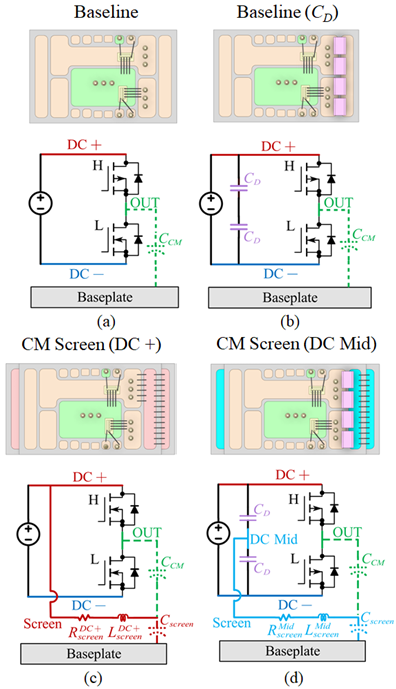
- Source: Caused by the rapidly changing voltage (high
dV/dt) on the switching nodes (e.g., the drain of the MOSFET). - Path: This is a "sneak path." The high
dV/dtcouples capacitively through parasitic capacitances to a common reference plane like the chassis or earth ground. The noise current then travels to the power source and returns through both the Line and Neutral conductors, flowing in the same direction. - Key Parasitics: The most significant parasitic paths for your PCB review work are:
- Capacitance between the MOSFET's drain tab and its heatsink.
- Inter-winding capacitance within the main transformer or inductor.
- Capacitance from any PCB trace with high
dV/dtto a nearby ground plane or chassis.
CM noise is often more difficult to manage because it involves these unintentional, "parasitic" components that are not drawn on the schematic but are a physical reality of the layout.
The following segment of the video provides a detailed look at how common mode noise is generated and how it travels.
Powerful Knowledge 18 - EMI in power electronics
Let's dive deeper into the generation of common mode noise, which is often the trickiest to solve.
Please watch the segment from 40:34 to 50:10. Focus on the explanation of how the high dV/dt on the switching device pumps current through parasitic capacitance (e.g., to a heatsink or in the transformer) into Earth. The key takeaway is how a few picofarads of unintended capacitance can cause an EMI failure.
Test your understanding!
You are reviewing a PCB layout for a hard-switched converter. You notice that a large, unshielded heatsink for the main MOSFET is placed very close to the metal enclosure of the product, which is connected to earth ground. Which type of EMI are you most concerned about this feature making worse, and why?
Show answer
This feature is a major concern for Common Mode (CM) noise.
The MOSFET's drain, which experiences very high dV/dt, is thermally connected to the heatsink. The heatsink and the earthed metal enclosure form a capacitor. The fast-changing voltage on the heatsink will inject current through this parasitic capacitance into the earth ground, creating a significant common mode current loop.
The Impacts of EMI: Why We Care
Now that we know the sources, let's discuss why EMI is such a critical issue.
-
Regulatory Compliance: This is the most significant commercial impact. Products sold in major markets (US, Europe, etc.) must pass standardized EMI tests. A product that fails its EMI test cannot be legally sold. These tests measure the conducted and radiated noise from a device to ensure it doesn't interfere with other equipment, like radio communications. The test uses a Line Impedance Stabilization Network (LISN) to provide a standard impedance and to couple the noise to a spectrum analyzer, which plots noise amplitude versus frequency against a strict limit line. A failure late in the development cycle can be extremely costly and cause major project delays.
-
System Malfunction: High-frequency noise can cause serious functional problems.
- Self-interference: Noise can couple back into the power supply's own controller, corrupting sensor readings or causing erratic gate drive signals, leading to instability or even failure.
- Interference with other systems: The noise can disrupt the operation of nearby electronics. Imagine a medical device's power supply causing noise that interferes with a sensitive patient monitor, or an industrial converter disrupting a delicate control network.
As you can see, managing EMI is not an afterthought; it's a fundamental requirement of power supply design.
Conclusion
This lesson completes our tour of the problems inherent in hard switching. By adding EMI to the power loss we calculated previously, we have a full picture of the challenges.
Key Takeaways:
- The root source of EMI in hard-switched converters is the high rate of change of voltage (
dV/dt) and current (di/dt). - This noise propagates as Differential Mode (DM) noise, driven by switching current, and Common Mode (CM) noise, driven by switching voltage coupling through parasitic capacitance.
- CM noise is often harder to mitigate as it relies on unintentional physical paths related to PCB layout, component placement, and heatsinking.
- The impacts of EMI are severe, ranging from costly regulatory test failures to unreliable system operation.
We have now thoroughly defined the "hard switching problem." The next module begins our journey into the solution. In the next lesson, we will formally define zero voltage switching (ZVS) and explore the core principle of how using a resonant tank allows a switch to turn on with zero voltage across it, elegantly solving the capacitive turn-on loss and dramatically reducing the dV/dt that generates so much EMI.