Hello! Welcome to the final lesson in our module on the principles of Zero Voltage Switching.
In the last lesson, we established the three key conditions for achieving ZVS. The most critical of these, especially for practical applications, was the need for sufficient resonant energy. We saw that the inductor must carry a minimum current to store enough energy to fully discharge the switch's capacitance. This directly implies that ZVS performance is dependent on the load current and can be lost at light loads.
This raises a crucial question for designers: How can we maintain the benefits of ZVS across a wide range of operating conditions, especially at light load? Today's lesson will answer that by focusing on your final learning outcome for this module: to explain the trade-off between the ZVS operational range and circulating current losses.
Understanding this trade-off is fundamental to your goal of reviewing and optimizing power converter designs. It reveals the compromises that are made to extend the benefits of ZVS and helps you identify why a seemingly efficient topology might perform poorly under certain conditions.
The Problem and a "Forced" Solution
Let's start by seeing exactly what happens when we try to force a converter into ZVS. As we've discussed, a standard hard-switched converter can sometimes achieve ZVS "accidentally" at light loads if the ripple current is large enough to become negative at the switching transition. But what if we want to guarantee ZVS at all loads?
The following video from a university course on resonant switching provides an excellent demonstration. The instructor starts with a standard hard-switched buck converter, which suffers from high switching losses. Then, simply by reducing the inductor value, he forces the inductor current to have a much larger ripple, ensuring it goes negative even at full load. This negative current provides the energy needed for the ZVS transition.
ECEN 5817 Resonant and Soft Switching Techniques in Power Electronics - Sample Lecture
This segment from a lecture by Prof. Dragan Maksimović at the University of Colorado Boulder demonstrates how altering a component value can induce ZVS.
Please watch from 27:57 to 37:25. Observe how changing the inductor from 100 µH to 10 µH creates a large ripple current that becomes negative. Pay close attention to the explanation of how this negative current enables the ZVS transition by charging and discharging the switch capacitances, eliminating the problematic turn-on power spike.
As you saw, forcing the inductor current to reverse direction at the switching instant successfully created the condition for ZVS, eliminating the large turn-on switching loss. The current that flows beyond what is required by the load, and which is used to enable the ZVS transition, is known as circulating current.
Defining Circulating Current and Its Cost
Circulating current is essentially energy that is shuttled back and forth within the converter's primary side but is not delivered to the output. Its sole purpose is to provide the energy for the ZVS resonant transition.
A more formal definition is provided in the following document.
Chapter 4 LLC Resonant Converter
This chapter on LLC converters provides a clear and concise definition of circulating energy, which is directly related to circulating current.
Please read the two paragraphs on page 98, starting from 'Operating region is on the right side...' down to '...the higher the conduction loss.'. Focus on the definition of circulating energy and its direct consequence on conduction loss.
The key insight is that while this circulating current eliminates turn-on switching losses, it is not "free." This extra current must flow through the MOSFETs, the inductor, and the interconnecting copper traces. Since all these components have some resistance ( for a MOSFET, DCR for an inductor), this larger total current leads to higher conduction losses, which are proportional to the square of the RMS current ().
This introduces the central trade-off of ZVS design.
The Core Trade-off: Switching Loss vs. Conduction Loss
We add circulating current to reduce switching losses, but in doing so, we increase conduction losses. A well-designed ZVS converter is one that carefully balances these two opposing loss mechanisms.
Let's return to the lecture video, which now analyzes the efficiency of the new "ZVS Quasi-Square-Wave" converter and compares it to the original hard-switched design.
ECEN 5817 Resonant and Soft Switching Techniques in Power Electronics - Sample Lecture
This next segment of the lecture directly analyzes the trade-off we've been discussing by comparing the losses in the different converter designs.
Please watch from 45:29 to 52:43. The instructor compares the power losses of the hard-switched converter against the two soft-switched versions. Notice his explanation for why the losses didn't decrease as much as expected: the switching losses went down, but the conduction losses went up due to the higher ripple (circulating) current. This is the most important takeaway of the lesson.
The video makes the point perfectly:
- You gain by eliminating turn-on switching losses.
- You lose by increasing conduction losses due to higher RMS current.
- You also lose by potentially increasing turn-off switching losses, as the MOSFET now has to turn off a larger peak current.
The net result depends on the specific operating point. At full load, the ZVS quasi-square-wave converter was the most efficient. However, at light load, the original hard-switched converter was the winner because it "naturally" achieved ZVS without needing the excessive circulating current of the other designs.
This highlights the fundamental challenge: a converter optimized for one operating point may be inefficient at another. A design paper from Vicor summarizes this trade-off beautifully.
High-Performance ZVS Buck Regulator Removes Barriers ...
The whitepaper 'High-Performance ZVS Buck Regulator' provides a very concise statement on this balancing act.
Please read the paragraph on page 7 that begins 'The figure shows the resonant transition ZVS action...'. Focus on the sentence that explicitly describes the trade-off.
As the paper states: "There is a tradeoff made to minimize the losses associated with clamp phase [circulating energy] versus the power savings by switching Q1 at exactly zero volts." Sometimes, accepting a small amount of switching loss (imperfect ZVS) is better than paying the heavy penalty of high circulating currents.
Test your understanding!
A designer has two ZVS converter designs for a battery-powered device that spends 90% of its time in a low-power sleep mode and 10% at full power.
- Design A: Uses a large resonant inductor, which creates very high circulating currents. It achieves perfect ZVS from 0% to 100% load.
- Design B: Uses a smaller resonant inductor. It achieves ZVS from 20% to 100% load but hard-switches in the sleep mode (e.g., at 5% load).
Which design is likely to result in longer overall battery life, and why?
Show answer
Design B is likely the better choice.
While Design A achieves ZVS at all times, the high circulating currents required to maintain ZVS in the low-power sleep mode would lead to significant and constant conduction losses. Since the device spends 90% of its time in this mode, these persistent conduction losses would likely outweigh the small switching losses incurred by Design B during that same period.
Design B makes a more practical trade-off: it accepts minor hard-switching losses in the mode where the device spends most of its time (and where currents are low anyway), in exchange for much lower conduction losses. It saves its ZVS capability for the high-power state where switching losses would be most significant.
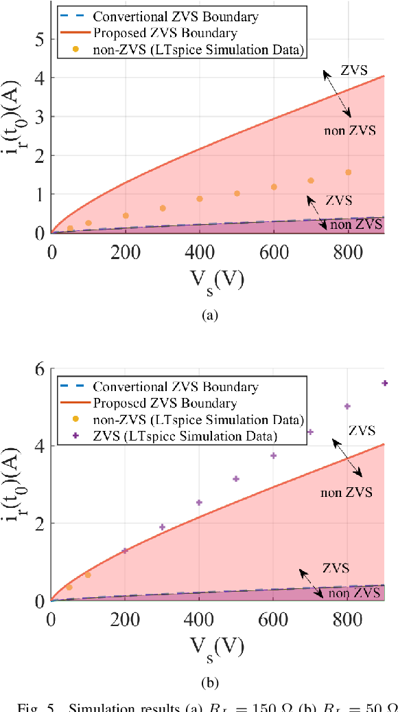
Visualizing the ZVS Operational Range
This trade-off defines the converter's ZVS operational range. Designers use circulating current to "push" the boundary of this range to cover the required load conditions. The goal is to ensure ZVS is active where it matters most (typically at higher loads and higher input voltages, where switching losses are dominant) without paying an excessive conduction loss penalty where it doesn't (at light loads).
Conclusion
In this lesson, you have explored one of the most important practical aspects of soft-switching design. You now have the conceptual tools to understand not just how ZVS works, but also the engineering compromises required to implement it effectively.
Key Takeaways:
- ZVS at light load requires circulating current: To ensure there is enough resonant energy when the load current is low, designers intentionally circulate extra current in the primary circuit.
- Circulating current causes conduction losses: This extra current increases the RMS current in the components, leading to higher losses, which can offset the gains from ZVS.
- The fundamental trade-off: ZVS design is a balance between reducing switching losses and increasing conduction losses. The optimal design depends on the specific application and its expected operating profile.
- Operational Range: The result of this trade-off defines the range of load and line conditions over which the converter can maintain ZVS.
You have now completed the module on the principles of ZVS! You've learned what it is, how a resonant tank enables it, the conditions required for it to work, and the critical trade-offs involved in its implementation.
In the next module, we will begin applying this knowledge to specific, common converter topologies. We'll start by applying ZVS to the familiar Buck and Boost converters, examining how ZVS is achieved in synchronous versions of these topologies and the practical challenges involved.