Hello! Welcome to the first lesson of our new module, where we start applying the principles of Zero Voltage Switching to specific converter topologies you'll encounter in practice.
In our last lesson, we explored the fundamental trade-off of ZVS design: the balance between eliminating switching losses and the penalty of increased conduction losses from circulating currents. We learned that to achieve ZVS, especially at light loads, we often need to force a negative current to flow at the switching instant, providing the energy to discharge the switch's capacitance.
Today, we'll see a clever and common way this is achieved in a synchronous buck converter. You'll learn how ZVS can be an almost "free" byproduct of the topology's normal operation. Our goal for this lesson is to explain how dead-time and body diode conduction enable ZVS in synchronous buck converters. This is a classic example of using parasitic elements and careful timing to gain a significant efficiency advantage, a key concept for your goal of optimizing PCB designs.
From Asynchronous to Synchronous Buck
You're already familiar with the standard buck converter, which uses a switch (a MOSFET) and a diode to step down voltage. To improve efficiency, especially in low-voltage, high-current applications, the diode is often replaced with a second MOSFET. This is called a synchronous buck converter.
- The top switch is the control FET or high-side switch.
- The bottom switch is the sync FET or low-side switch.
The main reason for this change is to reduce conduction losses. A MOSFET's on-resistance () typically creates a much smaller voltage drop than a diode's fixed forward voltage, leading to lower losses.
However, controlling two switches creates a new challenge: we must ensure they are never on at the same time. If they were, they would create a direct short circuit from the input voltage to ground, a condition called shoot-through, which is typically destructive.
Dead-Time: A Necessary Pause
To prevent shoot-through, controllers introduce a small delay in the switching sequence called dead-time. During this period, the controller commands both the high-side and low-side MOSFETs to be off.

During this dead-time, the inductor current () cannot instantaneously drop to zero. Since it's flowing out to the load, it must find an alternative path. That path is through the intrinsic body diode of the low-side MOSFET.
Body Diode Conduction: The Unsung Hero of ZVS
Every MOSFET contains a parasitic P-N junction between its source and drain that acts as a diode. This is the "body diode."
When the high-side switch turns off and the dead-time begins, the inductor current forces this body diode on, allowing current to continue flowing from ground to the switch node. This process is called body diode conduction or commutation.
This action has a crucial consequence: it clamps the switch node voltage to one diode drop below ground (e.g., -0.7 V).
Now, let's consider the full sequence that leads to ZVS for the more critical high-side switch. The process is a beautiful interplay between the inductor's energy and the switches' parasitic capacitances.
The following resource from Vishay provides an excellent, concise description of the sequence.
Beware of Zero Voltage Switching - Mouser Electronics
The application note 'Beware of Zero Voltage Switching' clearly explains the sequence of events in a synchronous buck converter that leads to ZVS.
Please read the section titled 'Synchronous Switching' on page 2. Then, continue to the next section and read the paragraph beginning 'In synchronous circuits...'. Pay close attention to the step-by-step 'sequence of current transfer' described. This sequence is the core mechanism we are studying.
Let's break down that sequence, focusing on achieving a zero-voltage turn-on for the high-side switch (Q1):
- Initial State: The low-side switch (Q2) is on, and inductor current is flowing. The switch node is held near ground.
- Q2 Turns Off: The controller turns off Q2. The dead-time interval begins.
- Resonant Transition: The inductor current, which cannot stop instantly, now has to go somewhere. It flows up into the switch node. This current charges the output capacitance () of Q2 and, crucially, discharges the output capacitance of Q1.
- VDS of Q1 Falls: If the inductor has sufficient energy, it will drive the switch node voltage all the way up from 0 V to the input voltage, . At this moment, the drain-to-source voltage () across Q1 has become 0 V.
- Body Diode Conduction (Q1): The inductor current continues to flow, slightly overshooting and forward-biasing the body diode of the high-side switch (Q1). This clamps Q1's at 0 V (or slightly positive).
- ZVS Turn-On: Now, with the voltage across Q1 already at zero, the controller applies the gate signal to turn it on. Since there is no voltage across the switch, the turn-on is lossless ().
This process happens in reverse to achieve ZVS for the low-side switch. When Q1 turns off, the inductor current discharges the switch node from down to 0 V, allowing Q2 to turn on at zero voltage after its body diode conducts.
The key takeaway is that the energy stored in the output inductor is used to charge and discharge the switches' parasitic capacitances during the dead-time, which is what enables ZVS.
Let's visualize this step-by-step.
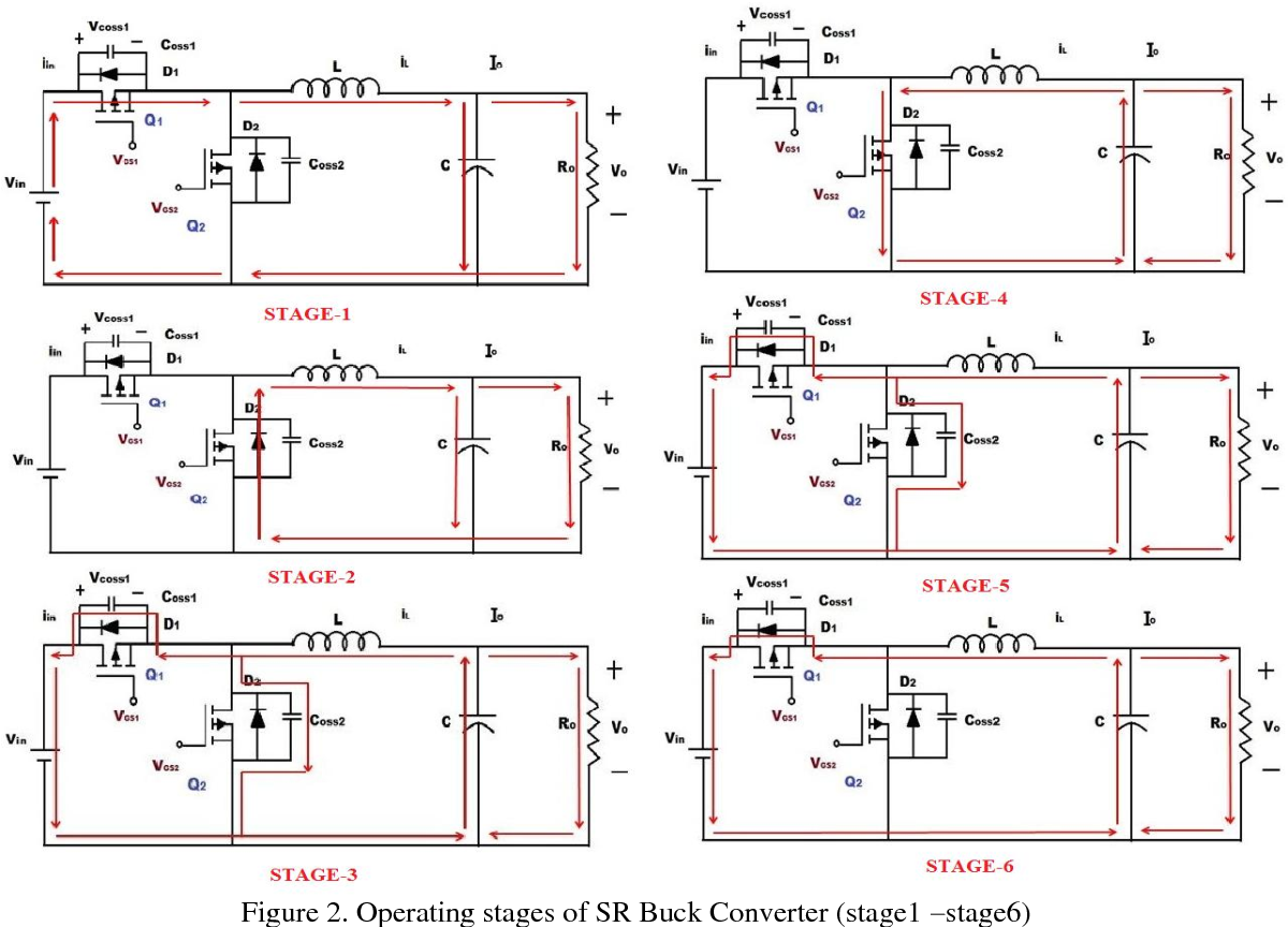
- Stage 5: Q2 is turned off. The inductor current
ILdrives the switch node voltage up, discharging Q1's capacitance (Coss1). - Stage 6: The switch node reaches
Vin, and the current forward-biases the body diode of Q1 (D1). Q1 can now be turned on with ZVS.
Test your understanding!
A designer is reviewing a synchronous buck converter PCB. They notice that at light loads, the efficiency is lower than expected. Probing the circuit, they see that the switch node voltage no longer swings fully from rail-to-rail (0V to Vin) during the dead-time before the high-side switch turns on.
Why does this lead to lower efficiency, and what fundamental condition for ZVS is no longer being met?
Show answer
The lower efficiency is due to the loss of ZVS. The switch node not swinging fully to means the high-side MOSFET's output capacitance () is not fully discharged before turn-on. When the switch turns on, the remaining energy in is dissipated as heat, re-introducing the hard-switching turn-on loss that ZVS is meant to eliminate.
The fundamental condition that is no longer being met is that there is not enough energy stored in the inductor at light load () to fully charge/discharge the switch node capacitances during the dead-time.
The Hidden Cost: Reverse Recovery
While body diode conduction is the key enabler for ZVS in this topology, it isn't without its own drawbacks. The body diode of a standard silicon MOSFET is a P-N junction, which suffers from a phenomenon called reverse recovery.
To understand this, let's look at what happens when the high-side switch (Q1) turns on while the low-side body diode (D2) is conducting.
How to GaN 015 Understanding the Impact of Dead time, QRR, and COSS
This video from EPC, although focused on GaN technology, provides an excellent explanation of the reverse recovery phenomenon in a synchronous buck converter.
Please watch the segment from 8:31 to 11:55. Focus on the explanation of what reverse recovery is and how it essentially creates a momentary 'shoot-through' condition. The key takeaway is that turning on the high-side switch forces a large, brief reverse current through the low-side body diode, causing additional losses.
As the video explains, when the high-side switch turns on, it must not only supply the inductor current but also provide a large, brief pulse of current to "sweep out" the stored charge in the low-side body diode before it can begin blocking voltage. This reverse recovery current () results in a significant loss event (), which is proportional to the input voltage.
This introduces another trade-off:
- Pro: Dead-time enables ZVS, eliminating capacitive turn-on loss.
- Con: Body diode conduction during dead-time leads to reverse recovery loss () and diode conduction loss ().
For this reason, optimizing the dead-time is critical. It must be long enough to allow the ZVS transition to complete, but short enough to minimize the time the body diode conducts, thereby reducing and conduction losses. This is why you'll often see datasheets for controllers and advanced MOSFETs (like GaN, which has zero ) heavily focused on dead-time management.
Conclusion
In this lesson, you've seen how a synchronous buck converter cleverly uses its inherent structure and a carefully managed dead-time to achieve ZVS without needing extra resonant components.
Key Takeaways:
- Synchronous converters replace the freewheeling diode with a MOSFET for higher efficiency.
- Dead-time is a necessary pause where both switches are off to prevent shoot-through.
- During dead-time, the inductor current flows through the body diode of one of the MOSFETs.
- This current flow provides the energy to discharge the parasitic capacitance of the opposing switch before it turns on, enabling ZVS.
- This mechanism comes with a cost: reverse recovery loss () and body diode conduction loss, making dead-time optimization crucial.
You now understand the most common method of achieving ZVS in low-voltage DC-DC converters. This is a design pattern you will frequently see when reviewing PCBs for applications like computer motherboards, graphics cards, and point-of-load converters.
In the next lesson, we will build directly on this by exploring the mathematical condition that determines whether ZVS is successful. We will identify the minimum load current condition for achieving ZVS in a synchronous buck converter.