Hello! Welcome to our case study module. Over the past nine modules, we've built a strong foundation, moving from the fundamentals of inductors and capacitors all the way to the nuanced role of snubber circuits in advanced ZVS designs. You've learned the why behind ZVS and the how of implementing it through good layout practices.
Now, it's time to put it all together. This lesson begins our practical case study, where we will apply everything you've learned to a sample PCB layout. Our goal today is to master the first step in any effective PCB review, which directly aligns with our learning outcome: Apply layout principles to trace and evaluate high-current power loops and gate drive paths on a sample PCB layout.
These two loops are the heart of any switched-mode power supply. The power loop handles high, fast-changing currents, making it a primary source of voltage stress and EMI. The gate drive loop delivers the high-speed signals that control the switches, making it highly sensitive to noise and parasitic inductance. Mastering their evaluation is the most critical skill for reviewing a power converter's design.
1. The Power Commutation Loop: The Epicenter of Switching
The first thing to identify on any power converter PCB is the high-current power loop, also known as the commutation loop. This is the path through which current rapidly switches, or "commutates," between different components.
Let's use a familiar buck converter as our model. When the high-side switch is on, current flows from the input capacitor, through the switch, to the inductor and output. When it turns off and the low-side switch (or diode) turns on, the inductor current circulates through the low-side switch. The loop that contains the components involved in this rapid switching of current is the critical one.
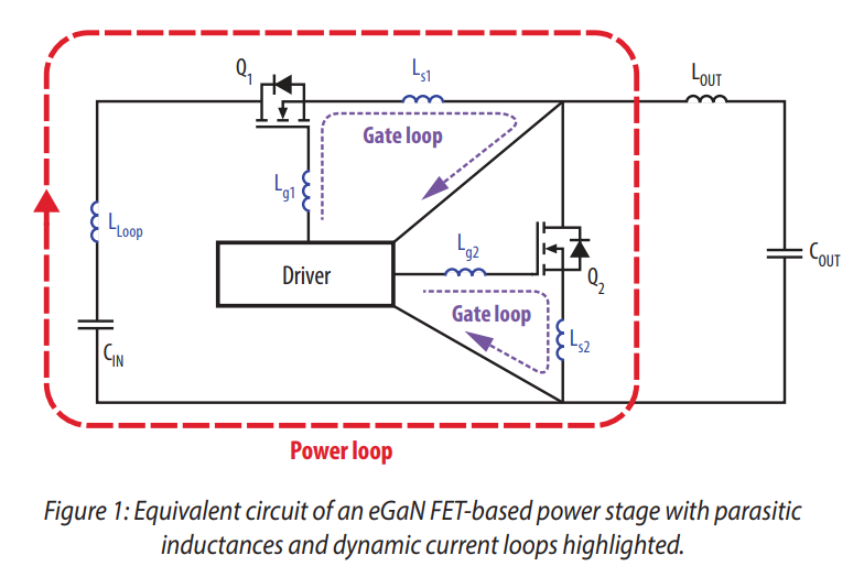
The area of this loop is the single most important parameter to minimize in a layout. As you know from basic physics, the inductance of a loop is proportional to the magnetic flux it encloses, which is directly related to its area. A large loop area means high parasitic inductance (). This inductance, when subjected to the very high rate of change of current () during switching, creates significant problems:
- Voltage Overshoot: A large voltage spike () appears across the switches, which can exceed their breakdown ratings.
- Ringing and EMI: The parasitic inductance resonates with parasitic capacitances, causing high-frequency ringing that radiates electromagnetic interference (EMI).
Identifying and Minimizing the Power Loop
To understand how to identify this loop and see the dramatic real-world effects of a poor layout, let's turn to an excellent lecture from MIT OpenCourseWare.
Lecture 38: Gate Drive, Level Shift, Layout
This video, "Lecture 38: Gate Drive, Level Shift, Layout," starts by clearly identifying the critical switching loop in a buck converter and then demonstrates the performance difference between a well-laid-out and poorly-laid-out board.
Please watch from 01:25 to 09:43. Focus on: How the presenter identifies the loop containing the input capacitor, switch, and diode as the critical high-frequency AC path. The four experimental waveforms showing the difference between good and bad layouts. Notice how a large loop area leads to severe ringing.
The key takeaway is that minimizing the physical area of this high-current loop is paramount. This is achieved by:
- Placing critical components close together: The input capacitor and the switches must be adjacent.
- Using short, wide traces: This reduces both resistance and inductance.
- Optimizing the return path: The path for the return current should be as close to the outbound current path as possible, but running in the opposite direction.
To see how these principles are applied in a modern PCB design tool, the following video provides a practical walkthrough.
(Sponsored) Switching Regulator PCB Design - Phil's Lab #60
The video "Switching Regulator PCB Design" by Phil's Lab gives a very clear, practical demonstration of how to place components for a buck converter to minimize critical loop areas.
Please watch from 02:14 to 17:19. Don't worry about replicating the steps in the software. Instead, focus on the reasoning behind the component placement decisions: Why is the input capacitor placed right next to the IC's input and ground pins? How is the inductor placed to keep the switching node (the connection between the switches and the inductor) small? Notice the priority: place the critical power components first, then route the less critical control signals.
The Physics of Loop Inductance
To solidify your understanding, it's helpful to connect these practical rules to the underlying physics. The concept of mutual inductance is key here. When you run a return current path directly underneath the forward path, their magnetic fields oppose each other, and the mutual inductance subtracts from the partial inductance of each trace, drastically reducing the total loop inductance. This is why using an adjacent ground plane layer for the return is so effective.
Optimizing PCB layout for HV CoolGaN™ power transistors
This application note from Infineon, "Optimizing PCB layout for HV CoolGaN™ power transistors," provides an excellent explanation of loop inductance and layout strategies. It's written for GaN, but the principles are universal.
Please read sections 4 ("Mutual and partial inductance") and 5 ("Package inductance: Is it a fixed value, or layout dependent?"). In section 4, focus on understanding how reducing the loop area (by flattening the loop) reduces inductance. In section 5, observe how different return path strategies (e.g., single-sided vs. double-sided return) around a thermal pad significantly change the total loop inductance. This demonstrates the trade-offs involved in a real layout.
2. The Gate Drive Loop: The Path of Control
Now let's turn to the second critical area: the gate drive loop. This is the path current follows to charge and discharge the MOSFET's gate capacitance, turning it on and off. The loop consists of the driver IC, the gate resistor, the MOSFET's gate and source terminals, and the return path to the driver's ground.
While the current is much lower than in the power loop, the loop's impedance is just as critical. Modern switches have low gate charge and turn on very quickly. This means the gate drive circuit must support high-frequency currents (often in the hundreds of MHz range). Any parasitic inductance in this loop forms an RLC circuit with the gate resistance and capacitance, causing several problems:
- Voltage Ringing: Overshoots on the gate voltage can damage the delicate gate oxide layer. Undershoots can cause the device to turn back on when it should be off.
- Slowed Switching: The
L * dI/dtvoltage drop across the loop inductance opposes the driver's output voltage, slowing down the turn-on and turn-off, which can increase switching losses. - Noise Susceptibility: A high-impedance gate loop is more susceptible to capacitively coupled noise (e.g., from the drain via the Miller capacitance), which can lead to spurious turn-on and shoot-through.
Key Concepts for Optimal Gate Drive Layout
The strategy for gate drive layout is very similar to the power loop: minimize the loop inductance. The Infineon application note we just looked at has an outstanding section on this.
Optimizing PCB layout for HV CoolGaN™ power transistors
Let's return to the Infineon application note. This section introduces the two most important concepts for achieving a low-inductance, noise-immune gate drive circuit.
Please read section 8.2, "The two key concepts for optimum gate-driver layout." This is a critical section. Pay close attention to: Key Concept #1: The comparison between a 'lateral loop' on one layer (Figure 14) and a 'vertical loop' using a return plane on an adjacent layer (Figure 15). Note the dramatic 5x reduction in estimated inductance. Key Concept #2: The idea that this return plane also acts as a shield, preventing noise from the high-voltage power stage from coupling into the sensitive gate circuit.
3. Application: Tracing a Sample PCB Layout
Now, let's apply these principles to a real-world example. Here is a PCB layout for an IGBT-based ZVS driver. Although it uses IGBTs, the layout principles for power and gate loops are identical to those for MOSFETs.

Let's evaluate it together.
1. Tracing the High-Current Power Loop:
- Components: The main power path involves the input terminals (VCC/GND), the bank of input capacitors (C1-C10), and the two IGBTs.
- Path: The high-frequency current will circulate from the positive terminals of the capacitors, through one of the IGBTs, out to the load (the primary of a transformer, connected at OUT 1/OUT 2), and return through the other IGBT to the capacitors' ground terminals.
- Evaluation:
- Proximity: The two IGBTs are placed symmetrically and relatively close. The input capacitor bank is also right next to the power switches. This is good.
- Loop Area: The main current path appears to be routed with large copper pours on the top layer. This creates a "lateral loop." While the traces are wide (good for current handling), the loop area is defined by the physical separation of the forward and return paths on that single layer. It's a reasonably compact lateral loop, but it's not as optimal as a vertical loop using an adjacent ground plane. The designer prioritized high current handling on a single layer.
2. Tracing the Gate Drive Loops:
- Components: You can see small resistors (like R1, R2) and diodes (FR207) placed very close to the gate pins of the IGBTs. These are the gate drive components.
- Path: A driver IC (not shown) would send a signal through these components to the gate of each IGBT. The return path for the gate current is from the IGBT's emitter (source, for a MOSFET) back to the driver IC's ground reference.
- Evaluation:
- Proximity: The gate drive components are placed right at the IGBT pins. This is excellent practice and minimizes the trace length from the final drive components to the gate itself.
- Loop: The traces for the gate signal and its return appear to be routed on the top layer. Similar to the power loop, this creates a lateral gate drive loop. Following Key Concept #1 from the Infineon note, this layout could be improved by placing a dedicated return plane for the gate drive circuit on an adjacent layer directly underneath these components. This would significantly lower the gate loop inductance and improve noise immunity.
Test your understanding!
Imagine you are reviewing the layout from the Phil's Lab video (LINK). A colleague suggests saving space by moving the input capacitor (C3) to the other side of the board, connecting it to the IC's input pin (pin 5) and ground pin (pin 2) with vias.
Based on what you've learned about power loops, why would this be a very bad idea?
Show answer
This would be a very bad idea because it dramatically increases the area, and therefore the inductance, of the most critical high-current switching loop.
-
Increased Loop Area: The current would have to travel from the IC's input pin, down through a via, across a trace on the bottom layer to the capacitor, back through another trace, up through another via to the ground pin. This creates a large physical loop, both laterally and vertically, massively increasing the parasitic inductance (
L_p). -
Consequences: As seen in the MIT video, this high
L_pwould interact with the fastdI/dtof the switching current, causing severe voltage spikes across the internal switch and massive high-frequency ringing. This would increase component stress, likely leading to failure, and generate significant EMI that could disrupt the entire system. The fundamental rule is to keep the high-frequency decoupling capacitor as close as physically possible to the switch and its return path, on the same layer if possible.
Conclusion
In this lesson, you've taken the first and most important step in practical PCB review by learning how to trace and evaluate the two most critical current paths in any ZVS converter.
Key Takeaways:
- Find the Loops First: The first step in a PCB review is to identify the main power commutation loop and the gate drive loops.
- Power Loop Goal: Minimize Area. A tight power loop with minimal area is essential to reduce parasitic inductance, which in turn minimizes voltage overshoot and EMI. This is best achieved by co-locating input capacitors and switches and using an adjacent plane for the return current.
- Gate Drive Loop Goal: Minimize Inductance & Shield. A low-inductance gate loop ensures clean, fast switching. This is best achieved by placing driver components close to the switch and using a dedicated return plane directly beneath the gate drive circuit, which also serves as a shield.
- Layout is a Game of Trade-offs: As seen in the examples, perfect optimization of one loop might conflict with another (e.g., thermal requirements vs. power loop return paths). Recognizing and evaluating these trade-offs is the mark of an experienced reviewer.
In our next lesson, we will continue our case study by examining other critical layout features. We'll look at how to identify aspects of the layout that could compromise ZVS operation, such as parasitic capacitance on the switching node, and how to trace sensitive analog feedback paths to ensure they are protected from noise.