Hello! Welcome to the final lesson in our case study on ZVS converter review.
In the last two lessons, we've done a deep dive into the physical PCB layout. We learned how to trace the critical power and gate drive loops, and how to spot subtle layout features—like an oversized switching node or a broken ground plane—that can radiate noise and prevent a converter from working correctly.
However, a perfect layout can't rescue a design that uses the wrong components. The ability of a converter to achieve Zero Voltage Switching is fundamentally determined by the characteristics of the switches and resonant parts chosen on the schematic.
Today, we shift our focus from the physical board to the electrical schematic. Our goal is to evaluate whether the component selections are appropriate for the intended ZVS operating range. By the end of this lesson, you'll have a practical checklist to assess if the chosen MOSFETs and resonant components are up to the task of delivering efficient ZVS performance.
1. The ZVS System: A Partnership of Components
Achieving ZVS isn't the job of a single component. It's a carefully choreographed "dance" between the switching elements (the MOSFETs) and the energy storage elements (the resonant inductor and capacitor).
- The MOSFETs: They introduce the parasitic output capacitance (Coss), which is the very capacitance we aim to discharge to zero before turn-on. Their intrinsic body diodes also play a crucial role in conducting current during the dead time.
- The Resonant Tank: The main inductor and capacitor form a resonant circuit. It's the energy stored in this tank, specifically the inductor, that must be sufficient to charge and discharge the MOSFETs' parasitic capacitances during the switching transitions.
You saw a clear example of this partnership in a previous module. Let's briefly recall that concept.
ECEN 5817 Resonant and Soft Switching Techniques in Power Electronics - Sample Lecture
Remember this segment from the ECEN 5817 lecture? It provides a powerful demonstration of how changing just one component—the inductor—fundamentally alters the circuit's behavior to enable ZVS.
Please watch from 27:57 to 33:10. You don't need to re-watch the whole thing, but refresh your memory on the core idea: reducing the inductor value increased the current ripple. This ensured the inductor current was negative at the switching transition, which provided the energy needed to discharge the switch capacitance and achieve ZVS, magically eliminating the turn-on loss spike.
This illustrates the core principle: for ZVS to work, there must be enough inductive energy available at the switching instant to overcome the capacitive energy stored in the switches. Your job as a reviewer is to check if the chosen components facilitate this energy transfer efficiently and reliably.
2. Evaluating the MOSFET: A Datasheet Deep Dive
When reviewing a schematic, the MOSFET datasheet is your primary source of truth. For ZVS applications, you aren't just looking for voltage and current ratings. You need to scrutinize three key parameters that dictate ZVS performance.
a) Output Capacitance (Coss) and Dead Time
The output capacitance, , is the capacitance across the MOSFET's drain and source terminals. To achieve ZVS, this capacitance must be fully discharged to zero volts during the dead time, before the MOSFET's gate is driven high.
The challenge is that is highly non-linear; it changes dramatically with the voltage across it.
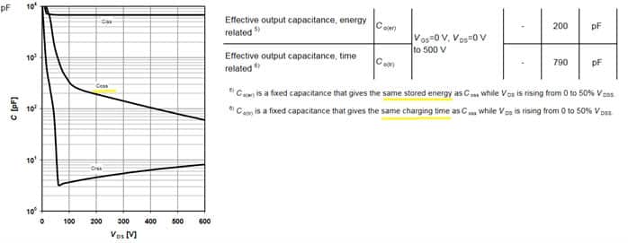
To simplify analysis, manufacturers provide effective capacitance values. The most useful for us is the time-related effective output capacitance, . This value represents a fixed capacitance that would take the same amount of time to charge as the real, non-linear .
This parameter directly connects to the required dead time. The following resource explains this relationship.
CoolMOS™ Primary Side MOSFET Selection for LLC ...
This application note from Infineon provides excellent detail on MOSFET selection for LLC converters, but the principles apply broadly to ZVS.
Please read section 2.2 The effect of dead time (page 5). Focus on equation (4) and the paragraph that follows it.
As the note explains, the minimum dead time required to discharge the capacitance is given by:
Note: This is for a half-bridge topology, hence the 2 * Co(tr) covering both switches' capacitances.
What this means for a reviewer:
When comparing two MOSFETs, the one with a lower is generally better for ZVS. It requires either less current or less dead time to achieve the transition, leading to a more robust and efficient design. You should check that the dead time programmed into the controller IC is sufficient for the chosen MOSFET's and the expected minimum magnetizing/resonant current.
b) The Body Diode: Friend and Foe
The body diode is an intrinsic part of a MOSFET's structure. In ZVS, it plays a friendly role: after is discharged, the inductor current flows through the body diode of the incoming MOSFET, clamping the voltage across the switch to near-zero. This provides a perfect window for a zero-voltage turn-on.
The danger comes from its reverse recovery characteristic. When a diode has been conducting, it stores some charge. To turn it off (i.e., make it block voltage again), this charge must be removed. If the other MOSFET in the half-bridge leg turns on before this diode has recovered, you create a momentary short-circuit, or "shoot-through," which can cause extreme current spikes, high losses, and device failure.
Zero-Voltage Switching Full-Bridge Converter
This application note from Vishay clearly explains the critical importance of the body diode and its recovery behavior.
Please read the section IMPORTANCE OF MOSFET BODY DIODE IN ZVS CIRCUITS. Pay close attention to the explanation of "shoot through" and the comparison of standard vs. Fast Body Diode (FBD) MOSFETs.
What this means for a reviewer:
For high-voltage ZVS converters, using a standard MOSFET is risky. You should explicitly check if the designer has chosen a MOSFET with a fast recovery body diode.
- Part Number: Look for suffixes like 'F', 'EF', or 'CFD' in the part number (e.g., SiHG47N60EF or CoolMOS™ CFD). This is the quickest indicator.
- Datasheet: Look for the Reverse Recovery Charge () and Reverse Recovery Time (). A fast diode will have a that is 5-10 times lower than a standard MOSFET of the same rating (e.g., 1.1 µC vs. 11 µC in the example from the text). A low is a critical requirement for reliability.
c) On-Resistance ()
Since ZVS virtually eliminates turn-on switching losses, conduction losses become a much larger portion of the total loss budget. Conduction loss is given by .
Therefore, selecting a MOSFET with a low is crucial for achieving high efficiency.
However, there is a trade-off. A device with a lower typically has a larger silicon die, which often leads to higher parasitic capacitances () and gate charge (). This can make achieving ZVS more difficult or increase other losses. A good design strikes a balance.
3. Practical Application: A Review Checklist
Let's synthesize these points into a practical process. Imagine you're reviewing a 2 kW power supply schematic that uses a ZVS Full-Bridge converter. How would you judge the MOSFET selection?
The Vishay application note provides a perfect, real-world example of this process.
Zero-Voltage Switching Full-Bridge Converter
This section walks through a concrete example of selecting a MOSFET for a ZVS full-bridge, starting from the power requirements and working down to a specific part number.
Please read the section ESTIMATION EXAMPLE USING CONDUCTION AND SWITCHING LOSSES AS 50/50. Follow the calculation steps.
Let's break down the logic:
- Define Requirements: The design is a 2 kW supply running from a 390 V input.
- Calculate Current: The RMS current through each MOSFET is calculated to be 4.49 A.
- Set a Loss Budget: The designer sets a target of 5 W for conduction losses per device.
- Determine Max : Using the conduction loss formula, they solve for the maximum allowable on-resistance.
(Note: The TCR, or Temperature Coefficient of Resistance, accounts for the fact that increases with temperature. A TCR of 2.0 is a conservative estimate for operation at 100°C.) - Check the Component: The chosen part is the SiHP28N60EF. Its datasheet typical is 107 mΩ, which is below the 124 mΩ limit. Good.
- Final Check: The 'EF' suffix confirms it has a fast body diode. The selection is appropriate.
Test your understanding!
A designer proposes using a standard (non-FBD) MOSFET for a 1 MHz ZVS converter. The MOSFET has an exceptionally low and the designer argues that this will maximize efficiency. Based on what you've learned, what is the primary risk with this choice, especially at such a high frequency?
Show answer
The primary risk is shoot-through and device failure due to incomplete body diode reverse recovery. A standard MOSFET has high and long . At 1 MHz, the switching period is only 1 µs, and the dead time will be a fraction of that (likely tens or a few hundred nanoseconds). There is a very high probability that the body diode will not have time to recover and regain its voltage-blocking capability before the opposing MOSFET in the leg turns on. This will cause catastrophic failure. The efficiency benefit of the low is irrelevant if the converter is unreliable.
Conclusion
Evaluating components on a schematic is a crucial step in PCB review, complementing the physical layout analysis. You're not redesigning the circuit, but you are performing a critical sanity check to catch potential issues before they become hardware failures.
Key Takeaways:
- ZVS is a System Property: Success depends on the interplay between the MOSFET's characteristics and the energy provided by the resonant tank.
- Focus on Key MOSFET Specs: When reviewing a schematic for a ZVS converter, prioritize these datasheet parameters:
- (Time-Related Output Capacitance): Lower is better. It determines the dead time needed to achieve ZVS.
- (Reverse Recovery Charge): Lower is critical. Check for Fast Body Diode (FBD) variants to ensure reliability and prevent shoot-through.
- (On-Resistance): Lower is better for efficiency, as conduction losses dominate in ZVS converters.
- Perform a Sanity Check Calculation: As shown in the example, you can use the power requirements to estimate the necessary and verify if the chosen component is in the right ballpark.
This lesson concludes our case study module on PCB review. You've now learned to analyze a design from both the layout and schematic perspectives.
In our next module, "Practical Design, Optimization, and Comparison," we will build directly on these concepts. The first lesson will focus on identifying these same critical MOSFET and resonant component parameters, but from the perspective of a designer making the initial selection, not just a reviewer evaluating a completed design.