Hello! Welcome to the next lesson in our course on Zero Voltage Switching.
In our last two lessons, we saw how a synchronous buck converter can achieve ZVS quite elegantly. By ensuring the inductor current reverses direction, we could use its energy to naturally discharge the switch's capacitance, eliminating turn-on losses. We defined the specific load condition required for this to happen: .
Today, we shift our focus to the boost converter. You might assume that achieving ZVS here would be similar, but as we'll discover, the fundamental operation of a boost converter presents significant obstacles. Our goal is to describe the operational challenges and limitations of achieving ZVS in synchronous boost converters. This lesson is crucial for understanding why you might see very different and more complex soft-switching circuits for boost converters compared to buck converters on the PCBs you review.
The Problem: Hard Commutation in the Synchronous Boost
Let's start with a standard synchronous boost converter. The main switch (S1, low-side) turns on to store energy in the inductor. Then S1 turns off, and the synchronous rectifier (S2, high-side) turns on to deliver that energy to the output.
The problem lies in the transition where S2 turns off and S1 turns on.
- S2 turns off: The inductor current, which is always flowing towards the output, now has nowhere to go. During the dead-time between S2 turning off and S1 turning on, this current forward-biases the body diode of S1.
- S1 turns on: S1 is now asked to turn on while its own body diode is conducting. This means the full output voltage is across S2, and when S1 turns on, it effectively short-circuits the output through S2's body diode until it recovers.
This is the opposite of the helpful situation in the buck converter. Here, the inductor current flows in a direction that forces a hard turn-on and, even worse, causes a violent hard commutation of the high-side switch's body diode.
This hard commutation of the body diode is the single biggest challenge. Let's explore why it's so problematic.
Beware of Zero Voltage Switching
To understand the severity of the body diode issue, let's read an excerpt from a technical article by Vishay, a major component manufacturer. It explains the practical consequences of body diode recovery in synchronous circuits.
Please read the section titled 'Body Diode Hard Commutation in Synchronous Circuits'. You can find it by searching for the heading 'There are more serious considerations for MOSFETs operating in ZVS circuits...'. Focus on the description of what happens during hard commutation in a synchronous circuit and why this is particularly difficult for high-voltage devices.
As the article explains, the reverse recovery of the body diode creates a large current spike () that causes:
- High Power Loss: The main switch turns on with high voltage across it and a large current spike flowing through it.
- Voltage Spikes and Ringing: The rapid change in current interacting with parasitic inductances causes severe electromagnetic interference (EMI) and voltage stress on the components.
- Potential for Device Failure: In high-voltage circuits, the recovery process can be so violent it can destroy the MOSFET.
The article makes a critical point that directly impacts your work: this is why high-voltage synchronous boost converters are rare. For applications like Power Factor Correction (PFC), designers often use an asynchronous boost with a specialized Silicon Carbide (SiC) diode, which has virtually no reverse recovery, to avoid this exact problem.
Solution 1: Boundary Conduction Mode (BCM)
Since ZVS doesn't happen naturally, we must force it. One way is to operate the converter in Boundary Conduction Mode (BCM), also known as Critical Conduction Mode (CrM).
In BCM, the inductor current starts from zero, ramps up, and then ramps all the way back down to zero in every cycle. The key ZVS-enabling event happens the moment the inductor current hits zero. At this point, both switches are off, and the inductor is free to resonate with the parasitic output capacitances () of the switches.
If there's enough energy stored in the capacitors, this resonance can cause the voltage across the main switch (S1) to naturally "ring" down to zero. The controller can then turn S1 on with zero voltage across it.
This sounds like a good solution, but it comes with significant operational limitations.
Challenge: Variable Switching Frequency
In BCM, the time it takes for the inductor current to ramp up and down depends on the input voltage, output voltage, and load current. This means the switching frequency is not constant.
Analysis and Design of a High-Efficiency Boundary-Conduction-Mode Boost Converter
This research paper on a BCM boost converter for LED drivers clearly explains the challenges. Let's read the introduction and conclusion, which highlight the frequency variation problem.
First, read the last paragraph of the introduction (Section I), starting from 'The biggest problem with the BCM boost converter...'. Then, read the first paragraph of the conclusion (Section V). Both sections explicitly state that the variable switching frequency is a major drawback of the conventional BCM boost topology.
As the paper states, a wide-ranging switching frequency makes it extremely difficult to optimize the design. EMI filters, magnetic components, and the control loop are all typically designed for a specific frequency. A variable frequency compromises performance across the board.
Challenge: ZVS is Not Guaranteed
The resonant ring that enables ZVS depends on having enough energy to swing the switch node voltage all the way to zero. Under some conditions, particularly light loads, there may not be enough energy.
The same paper illustrates this perfectly.
Analysis and Design of a High-Efficiency Boundary-Conduction-Mode Boost Converter
Let's look at the analysis of the soft-switching behavior in the same paper. It shows what happens when the resonance is too weak to achieve ZVS.
Please find Figure 9, 'Waveforms after tapped-inductor demagnetization.' The text explains that the solid line for the switch voltage (vds) shows a successful ZVS transition where the voltage rings down to zero. The dashed lines illustrate the case where ZVS is not achieved because the voltage fails to reach zero. This demonstrates the fragility of the ZVS condition in BCM.
If ZVS is lost, the converter reverts to hard switching, and all the associated losses and EMI problems return. This typically happens at light loads, which is ironic because that's often where you want high efficiency the most.
Solution 2: Zero Voltage Transition (ZVT) Auxiliary Circuits
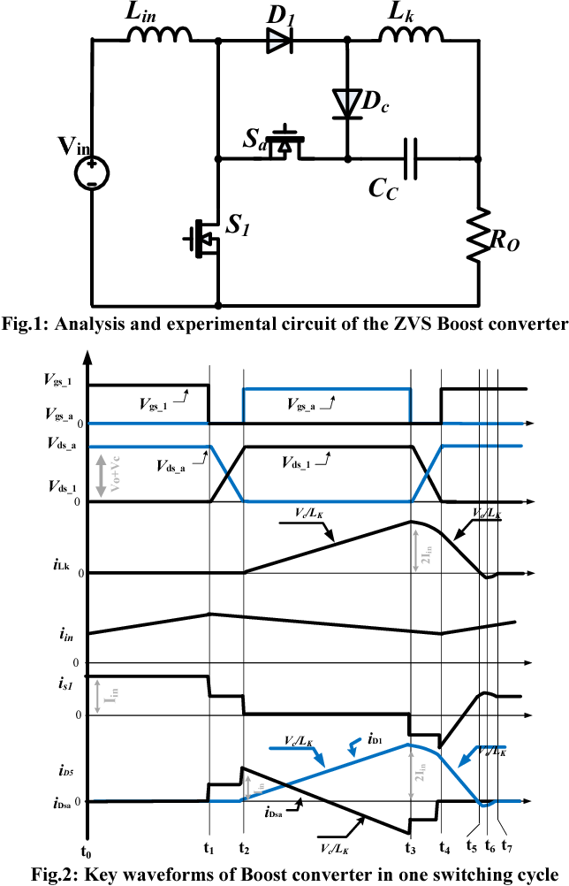
Another approach is to keep the main converter operating in a standard fixed-frequency mode but add a small auxiliary circuit to force ZVS. This is known as a Zero-Voltage-Transition (ZVT) converter.
The concept is quite clever.
Lecture 33: Soft Switching, Part 1
Let's watch a brief segment from an MIT OpenCourseWare lecture that introduces the ZVT boost converter concept.
Please watch from 47:09 to 50:18. The professor explains the core idea: a small, secondary circuit (the 'orange circuit') is added. Its only job is to turn on for a very short time right before the main switch turns on. It 'sucks the energy' off the main switch's capacitance, forcing its voltage to zero and enabling a soft turn-on. The main boost converter can then operate like a normal PWM converter.
Challenge: Complexity, Cost, and Size
The main limitation of the ZVT approach is obvious: you are adding more components. As the video and the diagram Analysis and experimental circuit of the ZVS Boost converter show, you need at least one extra (auxiliary) switch, an inductor, and a diode.
For you as a PCB reviewer, this means:
- Increased complexity in the control logic and layout.
- Higher bill-of-materials (BOM) cost.
- Larger PCB footprint.
While the ZVT circuit is usually low-power compared to the main stage, it's a significant design overhead that is only justified if the efficiency gains from eliminating switching losses are substantial.
Test your understanding!
You are comparing two PCB designs for a 48V output boost converter operating at 500 kHz.
- Design A is a standard synchronous boost converter.
- Design B is a ZVT synchronous boost converter with an auxiliary circuit.
Based on today's lesson, which design would you expect to have a better chance of functioning reliably and efficiently, and why? What is the main trade-off the designer of Design B has accepted?
Show answer
You would expect Design B (the ZVT converter) to be more reliable and efficient.
Reasoning: At 48V and 500 kHz, the hard commutation of the synchronous rectifier's body diode in Design A would be extremely problematic. This would lead to massive switching losses, severe EMI, and high voltage stress on the MOSFETs, potentially leading to failure. Design B uses the ZVT circuit specifically to eliminate these destructive turn-on losses, allowing for efficient and reliable high-frequency operation.
Trade-off: The designer of Design B has accepted the trade-off of increased cost, complexity, and board space in exchange for the higher efficiency and reliability that ZVS provides in this challenging application.
Conclusion
Achieving ZVS in a synchronous boost converter is fundamentally more challenging than in a synchronous buck. The topology does not lend itself to "free" soft switching.
Key Takeaways:
- The primary challenge is the hard commutation of the synchronous rectifier's (high-side) body diode during the main switch's turn-on, which causes severe losses, EMI, and stress.
- Operating in Boundary Conduction Mode (BCM) can enable ZVS through resonance, but this solution suffers from variable switching frequency and an unreliable ZVS range (often lost at light loads).
- Adding an auxiliary ZVT circuit can force ZVS in a standard fixed-frequency converter, but at the cost of increased complexity, size, and cost.
This explains why you will see these more complex BCM or ZVT implementations on boost converter PCBs, especially in high-frequency or high-voltage applications. The designers are actively fighting the converter's natural tendency to hard-switch.
In our next module, we'll begin exploring isolated converters, starting with one of the most common topologies in the industry: the flyback converter. We will learn its basic operating principles and then see how a clever technique called an "active clamp" can be used to achieve ZVS.