Hello! Welcome to the first lesson of your journey into embedded systems. Your goal is to build the expertise needed to work on complex, safety-critical systems at companies like SpaceX and Shield AI. This course is designed to bridge the gap between your computer science background and the specific demands of embedded engineering.
To start, we need a solid mental model of the hardware we'll be controlling. In this lesson, we will explore the high-level architecture of a modern microcontroller. You'll learn about its three fundamental components:
- The CPU core, which is the "brain" of the chip.
- The peripherals, which are the hardware modules that allow the chip to interact with the physical world.
- The memory map, which is the "address book" that organizes how the core communicates with memory and peripherals.
This foundational knowledge is the essential first step before we can start writing code to control hardware.
The Big Picture: What is a Microcontroller?
In your computer architecture courses, you studied general-purpose processors like those in laptops or servers. A microcontroller (MCU) is different; it's a complete computer on a single chip, designed specifically for control tasks in embedded systems.
Let's look at a typical structure.

This diagram shows the main idea: a central processing core (the Cortex-M4) is surrounded by a collection of specialized hardware blocks called peripherals. These are all connected by a system bus, which is an internal communication highway.
To formalize this, please read a short introduction on what makes a microcontroller distinct.
Lecture 14: - Microcontrollers & Memory-Mapped I/O
This excerpt from a university lecture series introduces microcontrollers and contrasts them with the microprocessors you might be more familiar with. It also highlights why the ARM Cortex-M family is so prevalent in the industry.
Please read the first few slides, starting from the definition of a microcontroller and continuing through the slide titled Cortex M-Series Microcontrollers.
The key takeaway is that a company like STMicroelectronics or NXP licenses the core design from ARM (the designer) and then integrates it with their own set of peripherals to create a final microcontroller product. The Cortex-M4 is a popular core, but it's part of a larger family.
This white paper from ARM provides a great overview of their Cortex-M processor family.
Read the initial overview and the section titled The Cortex-M Processor family (up to the last paragraph before section 1.3). This will give you a sense of where cores like the M0, M4, and M7 fit in terms of performance and features.
The Core: The "Brain" of the MCU
Now let's zoom in on the CPU itself. The core is responsible for executing your program's instructions. A Cortex-M core is more than just a CPU; it includes several tightly integrated components that are standard across all microcontrollers that use it.
This video gives an excellent walkthrough of the components that make up a Cortex-M4 core.
ARM Cortex-M4: Exploring The CPU | Embedded Systems podcast, in Pyjama!
This video explores the architecture of the ARM Cortex-M4 CPU.
Watch the section that describes the core's components. Pay attention to the distinction between standard and optional features.
As you saw, the core isn't just a raw processor. It includes critical subsystems like:
- CPU: The processor that runs the ARMv7-M instruction set.
- NVIC (Nested Vectored Interrupt Controller): A sophisticated interrupt manager. We'll dedicate a whole module to this later, but for now, know that it's the hardware responsible for handling events from peripherals.
- SysTick Timer: A standard, 24-bit timer available on all Cortex-M devices, often used by operating systems for scheduling.
- Debug/Trace Hardware (DAP, ETM): Interfaces for programming and debugging the chip.
- Optional Components: A vendor can choose whether to include features like a Floating Point Unit (FPU) for faster math with non-integers, or a Memory Protection Unit (MPU) to enforce access rules for different parts of memory.
Programmer's Model: The Registers
From a programming perspective, the most immediate part of the core you interact with is its set of registers. Like any RISC processor, the Cortex-M is a load/store architecture, meaning most operations happen on data held in registers.
The following segment of the same video explains the register set.
ARM Cortex-M4: Exploring The CPU | Embedded Systems podcast, in Pyjama!
Continuing with the video on the Cortex-M4 core.
Watch the segments that discuss the general-purpose and special registers, and then the overview of the Program Status Register (PSR).
To summarize, the Cortex-M programmer's model gives you:
- General-Purpose Registers (R0-R12): Used for data manipulation and calculations.
- Special-Purpose Registers:
- R13 (Stack Pointer - SP): Points to the top of the current stack. The core actually has two stack pointers (Main and Process) to cleanly separate the operating system from user applications, a key feature for robust systems.
- R14 (Link Register - LR): Stores the return address when calling a function.
- R15 (Program Counter - PC): Always points to the address of the next instruction to be executed.
- Program Status Register (PSR): A special register that holds status flags about the result of recent operations (e.g., was the result zero? negative?), the current interrupt status, and other CPU state information.
This register set should feel conceptually familiar from your computer architecture studies. The key difference here is its direct application to controlling a single, self-contained system.
The Peripherals: The "Senses and Muscles"
The core is powerful, but it can't do anything without peripherals to connect it to the outside world. Think of peripherals as specialized employees, each hired to do one job very well. The core acts as the manager, configuring these employees and telling them when to act.
Referring back to the block diagram, you can see a variety of common peripherals:
- GPIO (General Purpose Input/Output): The simplest peripheral. It allows you to control individual digital pins as inputs (to read a button) or outputs (to blink an LED).
- Timers: Incredibly versatile hardware for generating precise delays, creating periodic events (interrupts), and producing signals like PWM to control motor speed or LED brightness.
- Communication Peripherals (UART, I²C, SPI, CAN): These implement standard protocols for sending and receiving data between your MCU and other chips, sensors, or computers.
- ADC (Analog-to-Digital Converter): Reads analog voltages from sensors (like a temperature sensor or potentiometer) and converts them into digital values the CPU can understand.
We will dedicate entire lessons to programming these peripherals later in the course. For now, the important thing is to recognize them as the hardware interfaces for your software.
The Memory Map: The "Address Book"
So, we have a core that executes code and a set of peripherals that interact with the world. How does the core actually control the peripherals? The answer lies in the memory map.
An ARM Cortex-M processor has a unified 32-bit address space, meaning it can access up to 4 Gigabytes (2³²) of memory. This entire space is laid out according to a standard plan.
This video provides a fantastic visual explanation of the memory map concept.
Introduction to Cortex M0+ - Memory Map
This video provides an introduction to the memory map of a Cortex-M0+ processor. The fundamental concepts apply across the entire Cortex-M family.
Please watch the following segments: The overview of the 4GB memory space. The explanation of byte-addressable memory and how 32-bit data is handled. The breakdown of the different memory regions. The final segment illustrating how these regions are physically distributed but appear continuous to the CPU.
Here is a typical memory map diagram that visualizes this layout.
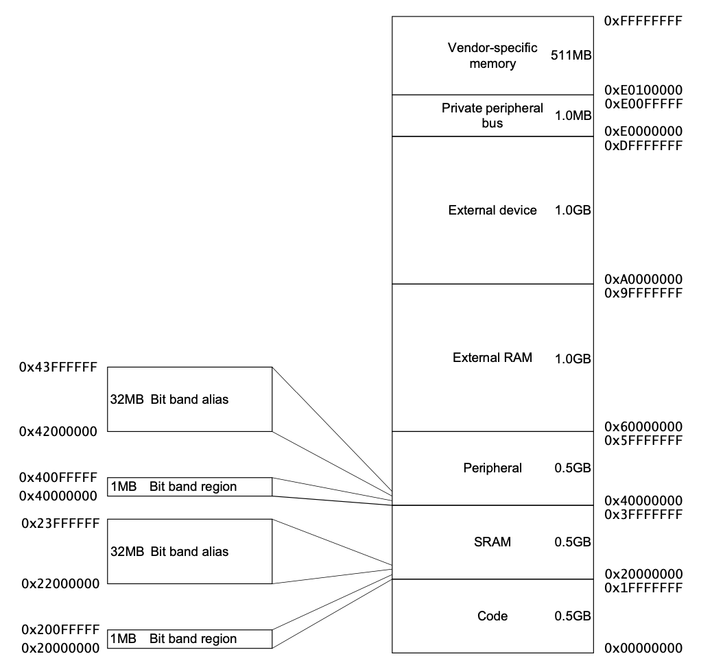
The key regions are:
- Code (Flash): This is where your program itself is stored. It's non-volatile memory, meaning it retains its content when the power is off. It's typically Flash memory.
- SRAM: This is the primary RAM for your application. It's used for read/write data, such as variables, and for the stack. It is volatile, so its contents are lost when power is removed.
- Peripheral: This is the crucial region for hardware control. Every function of every peripheral—its configuration, its status, the data it sends or receives—is controlled by special registers. These registers are "mapped" to specific addresses within this 0.5GB block.
- External RAM/Devices: These regions are for accessing memory or devices that are off-chip, such as an external SD card or an LCD screen.
This architecture leads to a powerful concept that is fundamental to all embedded programming: Memory-Mapped I/O.
Lecture 14: - Microcontrollers & Memory-Mapped I/O
This part of the lecture explicitly defines memory-mapped I/O and provides a table showing how peripheral registers are assigned to specific addresses.
First, read the brief explanation of Memory-Mapped I/O. Then, look at "Table 1. STM32F0xx peripheral register boundary addresses" on page 19 of the PDF. Notice how each peripheral, like GPIOA or GPIOB, has a specific range of addresses assigned to it.
The concept of memory-mapped I/O is where your C/C++ knowledge directly connects to hardware. To turn on an LED, you don't use a special instruction. You simply write a specific value to a specific memory address that corresponds to a GPIO peripheral's control register. Hardware control becomes an exercise in pointer manipulation, a concept that will be central to this course.
Conclusion
In this lesson, we've constructed a high-level mental model of an ARM Cortex-M microcontroller. Let's recap the key takeaways:
- A microcontroller is a self-contained computer on a chip, combining a CPU core with memory and peripherals.
- The ARM Cortex-M core is the "brain," featuring a set of general-purpose and special-purpose registers (PC, SP, LR) for executing code.
- Peripherals like GPIO, UART, and Timers are the "senses and muscles," enabling the microcontroller to interact with the physical world.
- The entire system is organized around a unified memory map, where specific address ranges are reserved for program code (Flash), data (SRAM), and hardware control (Peripherals).
- The mechanism for controlling hardware is memory-mapped I/O, where writing to or reading from specific memory addresses manipulates the peripheral control registers.
In our next lesson, we will get practical and learn how to navigate the official manufacturer documentation—the datasheet and reference manual—to find the exact addresses and bit-level details needed to control these peripherals.