Hello! Over the last two lessons, you have built the two fundamental computational blocks of a processor: a multi-bit ripple-carry adder for arithmetic, and a parallel logic unit for bitwise operations. You now have separate circuits for "A+B" and "A&B". But how does a computer choose which one to perform?
This lesson brings it all together. You will combine your adder and logic unit into a single, versatile component: the Arithmetic Logic Unit (ALU). This is the computational heart of the CPU, the circuit that does all the heavy lifting, from adding numbers to making logical decisions. You will learn the elegant design pattern that allows one circuit to perform many different functions, a principle that is central to computer architecture. The key, as you'll see, is a component you've already mastered: the multiplexer.
The ALU: One Unit, Many Operations
The core idea of the ALU is both powerful and surprisingly simple. Instead of building complex switching logic to reconfigure the circuit for every operation, we take a brute-force—and very fast—approach:
- Compute everything in parallel: We feed the input numbers (say, A and B) to all of our functional units at the same time. The adder calculates A+B, the AND gates calculate A&B, the OR gates calculate A|B, and so on. All of this happens simultaneously.
- Select the one result you need: All of these potential results are then fed into the inputs of a large multiplexer. A set of control wires, often called an opcode (operation code), is sent to the MUX's select lines. This opcode tells the MUX which one of the parallel results to pass through to the final output.
This design is incredibly efficient in terms of speed. There's no delay in "warming up" or reconfiguring a circuit for a specific task. By the time the control signals for the opcode are stable, the correct result is already calculated and simply needs to be selected.
The following article gives a great overview of the ALU's role and structure.
How an ALU Works: The Heart of CPU Architecture Explained | BIOS Confessions
This article from BIOS Confessions provides a clear, high-level introduction to the ALU, its purpose, and its construction.
First, read the introduction and the section "Arithmetic... what?" to understand the ALU's role as the central calculator of the CPU, combining an Arithmetic Unit (AU) and a Logic Unit (LU). Next, jump to the section on Control Signals. This part is crucial as it explains the core concept of using parallel computation and a multiplexer controlled by an opcode. Finally, read the section "Building a Simple 1-bit ALU". This will walk you through the design of a single "bit-slice," which is the fundamental building block for a larger ALU.
Designing the "Bit-Slice"
As you've seen in previous lessons and in the article, a common strategy for building circuits that operate on multi-bit numbers is the "bit-slice" architecture. We'll design a 1-bit ALU that can perform all our desired operations on a single pair of bits, and then we'll stack them to create a multi-bit ALU.
A 1-bit ALU takes two data inputs, A_i and B_i, and a carry-in, C_in (for the adder). It feeds them to a 1-bit full adder and a set of logic gates (AND, OR, XOR, etc.). The results from all of these components are then fed into a multiplexer. Control signals select the final output.
The diagram below shows a simple 1-bit ALU that can perform AND, OR, XOR, and ADD operations.

The M1M0 inputs are the opcode. For example:
- If
M1M0=00, the MUX might select theA&Bresult. - If
M1M0=01, the MUX might select theA|Bresult (the diagram shows NOR, but the principle is the same). - If
M1M0=10, the MUX might select theA^Bresult. - If
M1M0=11, the MUX might select the sum from the Full Adder.
To see this selection process illustrated clearly, the following video shows a diagram of the Hack computer's ALU. It uses the same principle of having an adder and an AND gate work in parallel, with a multiplexer choosing between them based on a control bit.
Nand2tetris with Diagrams (Part 7): ALU Implementation
This video provides a detailed walkthrough of the Nand2Tetris ALU design, with excellent diagrams showing the data flow.
Watch the segment from F control bit. Pay close attention to the diagram. You'll see the inputs x and y going to both a 16-bit Adder and a 16-bit AND unit. The control bit f acts as the selector for a multiplexer that chooses which of the two results proceeds to the next stage. This is the core concept of our ALU design in action.
From 1-bit Slice to 8-bit ALU
Now, let's scale up. To create an 8-bit ALU, we take eight of our 1-bit ALU slices and arrange them side-by-side. The wiring follows a clear pattern:
- Data Inputs: The 8-bit inputs
AandBare "sliced."A[0]andB[0]go to the first 1-bit ALU,A[1]andB[1]go to the second, and so on. - Control Inputs: The opcode bits are broadcast to every single slice. This is critical, as it ensures all 8 slices are performing the same operation (e.g., they are all doing an ADD, or they are all doing an AND).
- Carry Chain: For arithmetic operations, the
carry-outfrom one slice is connected to thecarry-inof the next slice, creating the same ripple-carry chain you built for your multi-bit adder. For logical operations, the carry chain is irrelevant. - Result Output: The 8 individual result bits from the slices form the final 8-bit ALU output.
The LogiSim tutorial you've seen before demonstrates this process perfectly. It first builds a 1-bit ALU and then combines eight of them into a full 8-bit ALU.
CSE 230 - LogiSim ALU Tutorial
This LogiSim tutorial shows the practical construction of an ALU, from a single bit-slice to a multi-bit unit.
First, re-watch the section on building the 1-bit ALU. Notice how the instructor places all the functional units (AND, OR, Adder, etc.) and uses a multiplexer to select the final result based on an operation input. This is a practical implementation of the bit-slice diagram you saw earlier. Now, watch the key part where he uses this 1-bit component to build an 8-bit ALU. Observe carefully how he: Uses a "splitter" to send A[0] and B[0] to the first slice, A[1] and B[1] to the second, etc. Connects a single multi-bit op input to all eight ALU slices. Chains the C_out of each slice to the C_in of the next to handle the ripple-carry for addition.
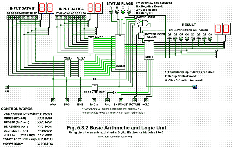
After this process, you have a complete ALU. The image below shows a slightly more complex but complete 8-bit ALU in a simulator, similar to what the video demonstrates. Notice the A and B data inputs, the CONTROL WORD (opcode) input, the final RESULT, and the STATUS FLAGS (like Zero, Carry, Negative), which provide information about the result of the last operation.
Conclusion
You have now reached a major milestone by combining the arithmetic and logic units into a fully-fledged ALU. This single component is the mathematical and logical engine of your entire computer. By understanding how to use multiplexers to select between operations performed in parallel, you've grasped one of the most fundamental design patterns in digital logic and computer architecture.
Key Takeaways:
- An Arithmetic Logic Unit (ALU) is a single combinational circuit that performs both arithmetic (e.g., ADD, SUB) and logical (e.g., AND, OR, XOR) operations.
- The standard ALU design involves computing all possible results in parallel and using a multiplexer to select the desired output.
- Control signals, collectively forming an opcode, are used to drive the select lines of the multiplexer, thereby "instructing" the ALU on which operation to perform.
- Multi-bit ALUs are constructed using a bit-slice architecture, where N identical 1-bit ALU slices are combined to create an N-bit ALU.
You have now completed the combinational logic section of your computer. You have a powerful calculator, but it has no memory. It can't store data or remember the state of a program. In the next module, "Sequential Logic and State," we will address this by introducing circuits that can hold a value over time, starting with the fundamental building block of all memory: the flip-flop.