In our previous lesson, we established the fundamental link between truth tables, Boolean expressions, and gate-level diagrams, learning how to convert between these three essential representations of a logic function. We saw that any function can be built using a combination of AND, OR, and NOT gates. Today, we will explore a powerful concept that revolutionizes how we think about building digital circuits: universal gates.
This lesson will introduce you to NAND and NOR gates and explain why they are called "universal." You will learn how to construct the three basic logic functions—NOT, AND, and OR—using only NAND gates or only NOR gates. Understanding this principle is not just a theoretical exercise; it has profound practical implications for integrated circuit design and manufacturing, simplifying the entire process from design to production.
What Makes a Gate "Universal"?
The set of gates {AND, OR, NOT} is considered functionally complete because any Boolean function can be expressed using them. A universal gate is a single type of gate that is, by itself, functionally complete. This means we can implement any logic circuit, no matter how complex, using only this one type of gate.
The two universal gates in digital logic are the NAND gate and the NOR gate. Let's briefly review them.
- NAND gate: The output is the complement of the AND operation. Its expression is . The output is
0only when all inputs are1. - NOR gate: The output is the complement of the OR operation. Its expression is . The output is
1only when all inputs are0.
To prove that NAND and NOR are universal, we simply need to show that we can create the three basic logic functions (NOT, AND, and OR) using only NAND gates, or only NOR gates.
The following video from Neso Academy provides a very clear and systematic proof of the universality of the NAND gate.
NAND Gate as Universal Gate (Part 1)
This video series from Neso Academy explains why the NAND gate is universal and demonstrates how to construct the basic logic gates from it.
First, watch the introduction which explains the strategy for proving universality from the beginning. Then, watch the implementation for each basic gate: NOT gate AND gate OR gate Pay close attention to how Boolean algebra, particularly De Morgan's laws, justifies these constructions.
Building with Universal Gates: A Deeper Look
Let's break down the implementations you just saw in the video. The key is to use Boolean algebra to verify each construction.
The Universality of NAND
As demonstrated, we can construct the three fundamental gates using only NAND gates.
-
NOT from NAND: By tying the inputs of a 2-input NAND gate together, we feed the same input
Ato both terminals. The output becomes . According to the idempotency law of Boolean algebra (), this simplifies to . -
AND from NAND: An AND gate is simply a NAND gate followed by an inverter. Since we can make an inverter from a NAND gate, we can construct an AND gate using two NAND gates. The output of the first gate is . This is then inverted by the second NAND gate, resulting in , which by the law of double complementation simplifies to .
-
OR from NAND: This is the most elegant construction and relies on De Morgan's laws. The expression for an OR gate is . By double complementing, we get . Applying De Morgan's law to the inner term gives . This expression can be directly implemented with NAND gates. We first generate and using two NAND gates as inverters. Then, we feed these into a third NAND gate.
The Universality of NOR
The same logic applies to the NOR gate. We can prove its universality by constructing the three basic gates.
-
NOT from NOR: Similar to NAND, tying the inputs of a NOR gate together gives an output of , which simplifies to ().
-
OR from NOR: An OR gate is a NOR gate followed by a NOR-based inverter. The first gate produces , and the second inverts it to , which equals .
-
AND from NOR: Again, we use De Morgan's laws. The expression for an AND gate is . Double complementing gives . Applying De Morgan's law gives . This is implemented by inverting the inputs
AandBwith NOR inverters and then feeding the results into a third NOR gate.
The image below provides a fantastic summary of all six of these basic implementations.

The following reading provides a detailed textual explanation and reinforces these concepts.
[PDF] Logic NAND Gate Tutorial
This document from a university course provides clear, concise sections on the universal properties of both NAND and NOR gates.
First, read the section The “Universal” NAND Gate. Then, find the section on the NOR gate and read The “Universal” NOR Gate. Compare the logic for both types of gates.
Why Is Universality Important?
You might be wondering why we would go to the trouble of building an AND gate out of two NAND gates when we could just use an AND gate. The reason is rooted in the practicalities of manufacturing and design.
From a manufacturing perspective, it is significantly more cost-effective and efficient to produce integrated circuits (ICs) using only one type of gate.
- Fabrication: The physical process of creating transistors and wiring them into a gate is complex. By using only one type of gate (e.g., NAND), the fabrication process only needs to be optimized for that single, repeatable structure.
- Inventory & Design: In the era of standard logic ICs (like the 74xx series), designers could stock up on one type of chip (e.g., the
7400Quad 2-input NAND gate) and use it for all their logic needs. This simplifies inventory management and the design process. Even in modern FPGA and ASIC design, the underlying logic cells are often based on universal structures.
Essentially, universality allows for immense simplification at the physical level, even if it seems to add a small layer of abstraction at the logical level.
Practice Problems
Let's apply these concepts. As you've requested, working through problems is one of the best ways to solidify your understanding.
Problem 1: Implement a function with NAND gates
Consider the Boolean function . Your task is to implement this function using only 2-input NAND gates.
Solution
-
Start with the original AND-OR circuit:
The function is an OR gate whose inputs areAand the output of an AND gate with inputsBandC. -
Replace each gate with its NAND equivalent:
- The AND gate () is replaced by a NAND gate followed by a NAND-inverter.
- The OR gate is replaced by a NAND gate with inverted inputs.
Let's combine these ideas. We can express the function using De Morgan's theorem to make it more NAND-friendly:
This looks like it can be implemented with NAND gates. -
Step-by-step construction:
- First, we need . This is a single NAND gate with inputs
BandC. - Next, we need . This is a NAND gate with its inputs tied to
A. - Finally, we feed and into a final NAND gate.
The circuit would look like this:
- Gate 1: Inputs
B,C. Output is . - Gate 2: Inputs
A,A. Output is . - Gate 3: Inputs , . Output is .
This implementation is correct. A common optimization is to notice that an OR gate can be implemented as a NAND gate with inverted inputs. So we need to feed
AandBCinto an OR gate. The NAND equivalent is to invertAandBCand feed them to a NAND gate. So:- Invert
Ato get (1 NAND gate). - Create
BCwith an AND gate (2 NAND gates). Inverting the output of this gives , which we don't want yet. We wantBC. So we use a NAND followed by a NAND inverter. - This seems complex. Let's try another approach using a double complement on the original expression: . This doesn't directly map to a simple NAND structure.
The most direct method is substituting the gate equivalents and simplifying.
- Start with the AND-OR circuit.
- Replace the AND gate with its 2-NAND equivalent.
- Replace the OR gate with its 3-NAND equivalent.
- This creates a messy circuit with lots of inverters. A key optimization trick (which you'll study in the next module) is to place two inverters (bubbles) in a row, as they cancel out. The final, optimized circuit for requires 3 NAND gates. We can see this if we redraw the OR gate as a negative-AND: an AND gate with inverted inputs.
The implementation is the most straightforward from the expression and requires three 2-input NAND gates.
- First, we need . This is a single NAND gate with inputs
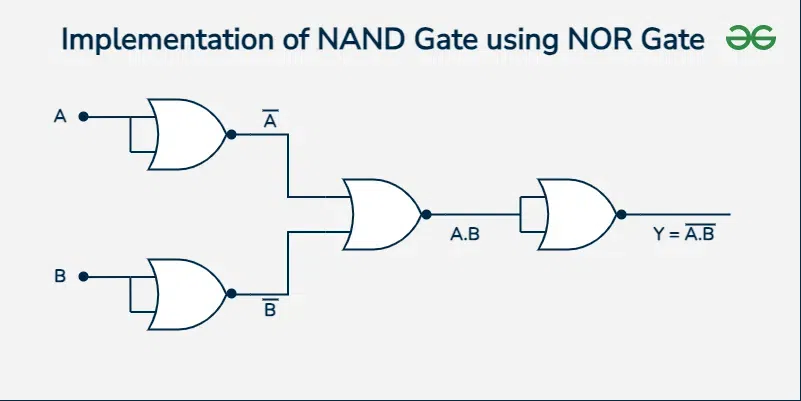
Problem 2: Convert between universal gates
How would you implement a 2-input NAND gate using only 2-input NOR gates? Draw the circuit diagram. (Hint: Think about the Boolean expression for NAND and how to create it with NORs).
Solution
-
Target Expression: The expression for a NAND gate is .
-
Use De Morgan's Law: Apply De Morgan's law to the expression: .
-
Plan the NOR implementation: This new expression looks very achievable with NOR gates.
- We need to generate and . We can do this using two NOR gates as inverters.
- Then, we need to OR these two results together. An OR gate can be built from a NOR gate followed by a NOR-inverter.
- Combining these, we feed and into a NOR gate. The output is , which simplifies to . This is an AND gate, not a NAND.
-
Rethink the strategy: We want . Let's start with the expression for an AND gate made from NORs: . To get NAND, we need to invert this entire expression.
So, the NAND function is equivalent to ORing the inverted inputs. This requires inverting A, inverting B, and then ORing them.- Invert A with a NOR gate: (1 NOR gate).
- Invert B with a NOR gate: (1 NOR gate).
- OR these two results () using an OR gate made of NORs (2 NOR gates).
This gives a total of 4 NOR gates. The circuit looks exactly like the one in this image:
Conclusion
In this lesson, you have learned the powerful concept of universal gates. This is a critical idea that bridges the gap between abstract Boolean logic and the physical reality of digital hardware.
Key Takeaways:
- NAND and NOR gates are universal gates because either one can be used to construct any possible logic circuit.
- To prove universality, we must show that we can create the basic NOT, AND, and OR functions.
- The constructions rely on Boolean algebra, particularly the idempotency laws and De Morgan's theorems.
- The primary advantage of universal gates is the simplification of manufacturing and design, allowing for efficient production of integrated circuits using a single, repeated gate structure.
We have now concluded our module on Boolean algebra and canonical forms. You have a solid grasp of how to manipulate and represent logical functions.
In the next module, we will dive into Combinational Logic Minimization Techniques. Now that we can build any function, the next logical question is: how can we build it using the fewest possible gates? You will learn powerful graphical (Karnaugh maps) and algorithmic (Quine-McCluskey) methods to simplify Boolean expressions. A key part of that process will be implementing these minimal expressions efficiently using the two-level NAND-only and NOR-only structures you were introduced to today.