Hello! Welcome to the third lesson in our module on Advanced Timers, PWM, and Signal Measurement.
In the last lesson, you mastered the crucial skill of calculating the Prescaler (PSC) and Auto-Reload Register (ARR) values to make a timer generate an update event at any desired frequency. This was a foundational step in precision timing.
Today, we will build directly on that knowledge to explore one of the most powerful features of STM32 timers: Pulse Width Modulation (PWM). Our learning outcome for this session is to configure a timer channel in Output Compare mode to generate a PWM signal. You'll see how the period you learned to calculate sets the PWM's frequency, and we'll introduce a new register that controls its duty cycle. PWM is essential in embedded systems for everything from controlling the brightness of an LED and the speed of a motor to generating audio signals, making it a cornerstone of your future work in automotive firmware and robotics.
1. The Principle of Timer-Based PWM
Let's start with the core concept. You already know how to make a timer's counter (CNT) repeatedly count from 0 up to the value in the ARR. This cycle's frequency is what you learned to calculate.
To generate a PWM signal, we introduce a third register: the Capture/Compare Register (CCRx). The timer hardware continuously compares the value of the CNT with the value in the CCRx. In its most common configuration (called PWM Mode 1), the logic is simple:
- If
CNT < CCRx, the output pin is HIGH. - If
CNT >= CCRx, the output pin is LOW.
The counter then continues until it reaches the ARR value, resets to 0, and the cycle begins again, bringing the output pin HIGH.
This relationship is perfectly illustrated in the following diagram.
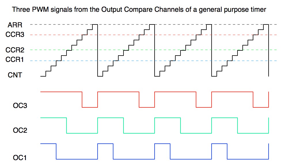
This gives us two simple, powerful formulas:
- PWM Frequency: Determined by the timer's overall period.
- PWM Duty Cycle: Determined by the ratio of the CCR value to the ARR value.
Before we dive into the registers, let's solidify this foundational knowledge.
STM32 PWM Tutorial | Timer PWM Signal Generation with HAL
The article 'STM32 PWM Tutorial' from ControllersTech provides a great overview of these concepts.
Please read the sections 'What is PWM (Pulse Width Modulation)?', 'STM32 Timer Overview for PWM', and 'Frequency and duty cycle basics'. Focus on how the article explains the relationship between the timer counter, ARR, and CCR, and make sure the formulas for frequency and duty cycle are clear.
2. Bare-Metal PWM Configuration: A Deep Dive
To meet professional standards, it's vital to understand how to configure peripherals by directly manipulating their registers. This gives you full control and a deeper understanding of the hardware. The following video provides an excellent, detailed walkthrough of this process using the reference manual. We will work through it in segments.
First, let's watch the conceptual overview which visualizes what we just discussed and introduces the idea of timer channels.
This first segment from Eddie Amaya's 'Stm32 Timers in PWM mode' video explains the relationship between the counter, ARR, and CCR to create a PWM signal.
Watch from 00:47 to 07:17. Pay close attention to the drawing that illustrates how the counter value rising to meet the CCR value dictates the 'on-time' of the signal. Also, note the point that a single timer can have multiple channels, all sharing the same frequency but capable of different duty cycles.
Now for the most critical part: configuring the specific registers. The next video segment walks through the reference manual to find the exact bits we need to set.
This segment is a masterclass in navigating a datasheet to configure a peripheral. It covers selecting the PWM mode and enabling preload registers for stable operation.
Watch from 07:17 to 18:25. Don't worry about memorizing every register name. Instead, focus on the process of how the presenter finds and interprets the required settings in the datasheet. Pay special attention to the concepts of PWM Mode 1 vs. Mode 2, and the purpose of the preload enable bits (OCxPE and ARPE).
Let's summarize the key register settings from that video for configuring a timer channel (let's say channel x) for PWM:
-
Configure the Channel as a PWM Output:
- In the
TIMx_CCMRxregister, set theOCxMbits to110for PWM Mode 1. - In the same
TIMx_CCMRxregister, set theOCxPE(Output Compare x Preload Enable) bit. This is crucial: it ensures that a new duty cycle value written to the CCRx register only takes effect at the next update event (when the counter resets), preventing glitches in the PWM output.
- In the
-
Enable the Channel Output:
- In the
TIMx_CCERregister, set theCCxE(Capture/Compare x Enable) bit. This connects the timer's internal PWM signal to the physical output pin.
- In the
-
Enable Auto-Reload Preloading:
- In the
TIMx_CR1register, set theARPE(Auto-Reload Preload Enable) bit. This applies the same preloading principle to theARRregister, ensuring smooth frequency changes.
- In the
-
Set the Timing Registers:
- Set the
PSCandARRregisters to get your desired frequency. - Set the
CCRxregister to get your desired duty cycle.
- Set the
-
Enable the Timer:
- In the
TIMx_CR1register, set theCEN(Counter Enable) bit to start the timer.
- In the
3. Practical Implementation
Let's put theory into practice. Your task is to write the bare-metal code to generate a 1 kHz PWM signal with a 25% duty cycle on pin PB9. On the Blue Pill, pin PB9 is connected to Timer 4, Channel 4 (TIM4_CH4).
Step 1: The Calculations
- System Clock: Your timer is clocked from the APB1 bus. If your system clock is 72 MHz, the APB1 clock is typically 36 MHz. However, for timers, there's a multiplier that often brings it back to 72 MHz. Let's assume a 72 MHz timer clock for our calculations.
- Frequency (1 kHz):
- We need
(PSC + 1) * (ARR + 1) = 72,000,000 / 1000 = 72,000. - Let's choose an
ARRthat makes duty cycle math easy. A good choice is999, soARR + 1 = 1000. - This means
PSC + 1 = 72,000 / 1000 = 72, soPSC = 71.
- We need
- Duty Cycle (25%):
CCRx = (ARR + 1) * (Duty Cycle / 100) = 1000 * (25 / 100) = 250.- We will write
250into theTIM4_CCR4register.
Step 2: Code Structure
Here is a C code structure. Your task is to complete the pwm_init() function by setting the appropriate bits in the registers we've discussed. Use the reference manual for your STM32F103 and the knowledge from the videos.
#include "stm32f10x.h"

void pwm_init(void) {
    // 1. Enable clock for GPIOB and TIM4
    RCC->APB2ENR |= RCC_APB2ENR_IOPBEN; // Enable GPIOB clock
    RCC->APB1ENR |= RCC_APB1ENR_TIM4EN; // Enable TIM4 clock

    // 2. Configure PB9 as Alternate Function Push-Pull
    // Clear any previous configurations for PB9 (CNF9[1:0] and MODE9[1:0])
    GPIOB->CRH &= ~(GPIO_CRH_CNF9 | GPIO_CRH_MODE9);
    // Set MODE9[1:0] to '11' (Output mode, max speed 50 MHz)
    GPIOB->CRH |= GPIO_CRH_MODE9;
    // Set CNF9[1:0] to '10' (Alternate function output Push-pull)
    GPIOB->CRH |= GPIO_CRH_CNF9_1;

    // 3. Configure TIM4 for PWM
    // Set Prescaler (PSC) and Auto-Reload Register (ARR)
    TIM4->PSC = 71;   // Results in 72,000,000 / 72 = 1,000,000 Hz (1 MHz) counter clock
    TIM4->ARR = 999;  // 1 MHz / 1000 = 1 kHz PWM frequency

    // 4. Set Duty Cycle in CCR4
    TIM4->CCR4 = 250; // (250 / 1000) * 100 = 25% duty cycle

    // 5. Configure PWM Mode for Channel 4
    // In TIM4_CCMR2, set OC4M bits to '110' for PWM Mode 1
    TIM4->CCMR2 |= (TIM_CCMR2_OC4M_2 | TIM_CCMR2_OC4M_1);
    // Enable Preload for CCR4
    TIM4->CCMR2 |= TIM_CCMR2_OC4PE;

    // 6. Enable the Channel 4 Output
    // In TIM4_CCER, set the CC4E bit
    TIM4->CCER |= TIM_CCER_CC4E;

    // 7. Enable the main output and counter
    // In TIM4_CR1, set the ARPE bit
    TIM4->CR1 |= TIM_CR1_ARPE;
    // In TIM4_CR1, set the CEN bit to start the timer
    TIM4->CR1 |= TIM_CR1_CEN;
}

int main(void) {
    pwm_init();

    while(1) {
        // The PWM is generated by hardware.
        // The CPU is free to do other tasks.
    }
}
Take your time to go through each line in the pwm_init function. Match the register names and bit masks to the concepts covered in the videos and the summary above. Compile this code and flash it to your Blue Pill. If you have an oscilloscope or a logic analyzer, connect it to pin PB9 to verify the 1 kHz frequency and 25% duty cycle.
Conclusion
Congratulations! You have successfully configured a hardware timer to generate a stable PWM signal using direct register access. This is a significant step towards professional embedded development.
Key Takeaways:
- PWM generation is a built-in feature of STM32 timers, operating in Output Compare mode.
- The timer's period, set by
PSCandARR, determines the PWM signal's frequency. - The Capture/Compare Register (
CCRx) value determines the PWM signal's duty cycle. - Correct configuration involves setting up the timer registers (
CCMRx,CCER,CR1) and the corresponding GPIO pin in Alternate Function mode. - Using preload registers (
OCxPEandARPE) is best practice for ensuring glitch-free updates to duty cycle and frequency.
Preview of the Next Lesson:
Our PWM signal is currently static. The real power of PWM comes from changing it dynamically. In our next lesson, we will programmatically control the duty cycle of a PWM signal to dim an LED. You will learn how to modify the CCRx register in real-time to create visible effects.