Hello! Welcome to your next lesson in our module on Advanced ARM Architectures.
In our previous session, we moved from theory to practice by writing the code to configure and enable an ARMv7 Memory Management Unit (MMU). We established a safe identity map and learned how to manipulate the key system control registers like TTBR0, DACR, and SCTLR. Enabling the MMU is often done in conjunction with enabling the data and instruction caches. Now that they are "on," we must learn how to manage them.
This lesson addresses a critical topic for any advanced embedded developer: implementing data cache maintenance operations (e.g., clean, invalidate) to ensure coherency. We will explore why this is necessary, what operations are available, and how to use them correctly. Your experience with ADAS communication stacks, which heavily rely on peripherals like DMA to move sensor data, makes this topic particularly relevant, as these are the exact scenarios where cache coherency problems arise.
The Problem: When Memory Lies
A cache improves performance by providing the CPU with a fast, local copy of main memory. This works perfectly as long as the CPU is the only component (or "bus master") changing that memory. However, in most embedded systems, other masters like a DMA controller, an Ethernet MAC, or another CPU core also access the same memory.
When this happens, the CPU's cached copy can become "stale" or out-of-sync with the actual main memory, leading to a loss of cache coherency. A system is cache-coherent if every master's view of a memory location is always the same.
Let's explore the two classic failure scenarios.
Managing Cache Coherency on Cortex-M7 Based MCUs
To visualize these problems, we will refer to a document from Microchip, 'Managing Cache Coherency on Cortex-M7 Based MCUs'. It clearly illustrates the two most common ways coherency is lost.
Please read Section 3, 'Cache Coherency Issues' (pages 4-5). Pay close attention to Figure 3-1 and Figure 3-2, which depict the two key scenarios we are about to discuss.
As you saw in the reading, the two main problems are:
-
DMA writes to memory, CPU reads from cache (Stale Read):
- A DMA controller receives data from a peripheral (e.g., a RADAR) and writes it into a buffer in SRAM.
- The CPU, which had previously accessed this buffer, holds an old copy of it in its data cache.
- When the CPU reads the buffer to process the new data, it gets a cache hit and reads the stale data from its cache, completely missing the new data written by the DMA.
-
CPU writes to cache, DMA reads from memory (Stale Read by DMA):
- The CPU prepares a data packet (e.g., a CAN message) in a buffer. With a write-back cache policy, this write only updates the local data cache, marking the cache line as "dirty". The data is not immediately written to SRAM.
- You then instruct the DMA to transmit this data.
- The DMA reads the buffer directly from SRAM and sends out the old, stale data, because the CPU's new data is still sitting in its cache.
The Solution: Manual Cache Maintenance
On processors without hardware coherency mechanisms (like many ARM Cortex-M7 or older Cortex-A/R cores), the software is responsible for manually fixing these situations using cache maintenance operations.
The two primary operations are:
- Invalidate: This tells the cache, "The copy of data you have for this memory range is potentially stale. Discard it." The next time the CPU needs to read from that address, it will be forced to fetch the fresh data from the main memory.
- Clean (also called Flush or Write-Back): This tells the cache, "The copy of data you have for this memory range is newer than what's in main memory. Write it back to main memory now." This makes the CPU's updates visible to other masters like the DMA.
A third operation, Clean and Invalidate, performs both actions. It writes the CPU's changes back to main memory and then discards the local copy.
Implementing Maintenance with CMSIS
The Cortex Microcontroller Software Interface Standard (CMSIS) provides a standard C API for these operations. Let's see how they solve our two scenarios.
Managing Cache Coherency on Cortex-M7 Based MCUs
The Microchip document also provides excellent C code examples showing exactly how and when to use these APIs. It also highlights a critical detail about memory alignment.
Please read Section 4, 'Using Cache Maintenance APIs to Handle Cache Coherency' (pages 6-11). Focus on the two main code examples: The scenario where the DMA writes to SRAM (using SCB_InvalidateDCache_by_Addr). The scenario where the DMA reads from SRAM (using SCB_CleanDCache_by_Addr). Also, pay very close attention to the 'Important' note and the final example that explains why buffer size and alignment are so critical.
Let's summarize the key implementation patterns.
Scenario 1: DMA writes, then CPU reads
To fix this, you must invalidate the cache range covering the buffer after the DMA has finished writing but before the CPU attempts to read it.
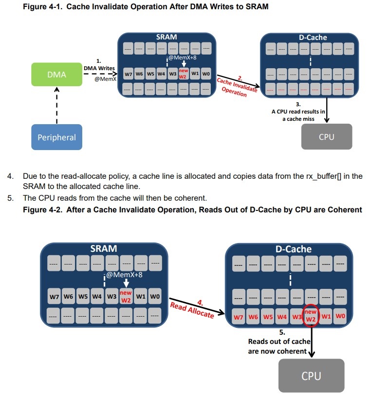
A typical implementation looks like this:
// Buffer must be aligned to the cache line size (e.g., 32 bytes)
__attribute__ ((aligned (32))) uint8_t rx_buffer[BUFFER_SIZE];

// In the DMA transfer complete interrupt service routine:
void XDMAC_Handler(void) {
    // ... DMA transfer is complete ...

    // Invalidate the cache region for rx_buffer before the CPU uses it.
    // This ensures the CPU will see the new data written by the DMA.
    SCB_InvalidateDCache_by_Addr((uint32_t*)rx_buffer, DMA_TRANSFER_SIZE);

    // Now it's safe for the main application to process rx_buffer.
    rx_xfer_done = true;
}
Scenario 2: CPU writes, then DMA reads
To fix this, you must clean the cache range covering the buffer after the CPU has finished preparing the data but before you start the DMA transfer.
// Buffer must be aligned to the cache line size (e.g., 32 bytes)
__attribute__ ((aligned (32))) uint8_t tx_buffer[BUFFER_SIZE];

void send_data_via_dma(void) {
    // 1. CPU prepares the data in the buffer.
    strcpy((char*)tx_buffer, "Data to be sent by DMA");

    // 2. Clean the cache for the buffer range.
    // This forces the new data from the D-Cache out to the main SRAM.
    SCB_CleanDCache_by_Addr((uint32_t*)tx_buffer, DMA_TRANSFER_SIZE);

    // 3. Now start the DMA. The DMA will read the correct, new data from SRAM.
    start_dma_transfer(tx_buffer, DMA_TRANSFER_SIZE);
}
A Critical Detail: Alignment
As the document stressed, cache maintenance operations work on entire cache lines (commonly 32 or 64 bytes). Your shared buffers must be aligned to a cache line boundary, and their size should ideally be a multiple of the cache line size. If not, cleaning or invalidating your buffer might accidentally corrupt adjacent data (like a status flag) that happens to share the same cache line. This is a subtle but common bug in embedded systems.
Test your understanding!
You are writing a driver for an automotive Ethernet peripheral. The driver uses DMA to move received network packets into a ring buffer of packet_t structs in SRAM. Your application code then pulls these structs from the buffer to parse them. To ensure coherency, where and what cache maintenance operation must you perform?
Show answer
This is the "DMA writes, CPU reads" scenario. After the DMA signals that it has finished writing one or more packets into the buffer, you must perform a cache invalidate operation on the memory region of the ring buffer that contains the new packets. This must be done before your application code attempts to read those packet_t structs. This ensures the CPU doesn't read stale data from its cache and instead fetches the fresh packets from SRAM.
The Deeper View: Barriers and Assembly
The CMSIS functions provide a convenient abstraction. Under the hood, they execute special processor instructions. On ARMv7-A/R processors, these are typically mcr instructions to the system control coprocessor (p15).

However, just issuing a cache maintenance instruction is not always enough. Modern processors can reorder instructions for efficiency. This means the CPU might execute an instruction that depends on the cache operation before the cache operation itself has actually completed.
To prevent this, we use memory barriers.
To understand barriers, let's look at an AArch64/ARMv8 tutorial. While the syntax is for ARMv8, the concepts of DSB, DMB, and ISB are fundamental to all modern ARM cores and essential for robust low-level programming.
Read the introductory section and the descriptions for the three barrier instructions: dsb, dmb, and isb. Focus on what each one guarantees.
The three key barriers are:
DSB(Data Synchronization Barrier): The workhorse for coherency. It's a "stop sign" for memory access. The CPU will halt and wait for all previous cache maintenance and memory access instructions to fully complete before executing any subsequent memory access instructions. You typically use aDSBright after a cache clean or invalidate operation to ensure it has finished before you, for example, enable a DMA transfer.DMB(Data Memory Barrier): A weaker barrier that only ensures the relative order of memory accesses. It's less common for simple cache coherency tasks.ISB(Instruction Synchronization Barrier): This barrier flushes the processor's instruction pipeline. It's used when the code itself has been changed (e.g., self-modifying code or loading a new program) to ensure the processor fetches the new instructions.
The canonical sequence for making a CPU-written buffer visible to a DMA is:
- CPU writes data to the buffer.
- Issue a Cache Clean operation.
- Issue a
DSBinstruction. - Start the DMA transfer.
The DSB guarantees that the clean operation is complete and the data is actually in main memory before the DMA is configured and starts trying to read it.
Synthesis: A Complex Coherency Problem
Let's look at a complex case that ties everything together: self-modifying code. This is where a program rewrites its own instructions. This requires ensuring coherency between the Data Cache (where the new instruction is written as data) and the Instruction Cache (from where it is fetched for execution).
The same tutorial provides a step-by-step walkthrough of how to correctly modify executable code in memory. This is the ultimate test of understanding cache and pipeline management.
Read the sections 'Self Modifying Code' and the subsequent section that builds the full instruction sequence. Follow the logic from simply storing the new instruction to adding the necessary dc, ic, and barrier instructions. This demonstrates a real-world application of these concepts.
The correct, robust sequence is:
STR w4, [x5]: Store the new instruction (w4) to the target memory address (x5). This updates the D-Cache.DC CVAU, x5: Clean the D-Cache line for that address. This pushes the new instruction from the D-Cache to main memory.DSB ISH: Data Synchronization Barrier. Ensures the clean operation completes before anything else happens.IC IVAU, x5: Invalidate the I-Cache line for that address. This removes the old, stale instruction from the I-Cache.DSB ISH: Another DSB is needed to ensure the I-Cache invalidation is seen by all parts of the pipeline.ISB: Instruction Synchronization Barrier. Flushes the pipeline, forcing the processor to re-fetch the instruction atx5, which will now be the new one.
This Clean -> DSB -> Invalidate -> ISB pattern is a fundamental recipe for managing coherency when code is modified.
Interview Corner
This topic is a staple in interviews for senior embedded roles. Expect questions that test both the "why" and the "how".
Q1: "What is a cache coherency problem? Describe a common scenario in an automotive system where it might occur."
A: "A cache coherency problem occurs when different bus masters, like the CPU and a DMA controller, have inconsistent views of the same memory location. A classic automotive scenario is with a CAN driver. The CPU prepares a CAN frame in a buffer in SRAM. If that buffer is cached and a write-back policy is used, the new data might only exist in the CPU's cache. If you then instruct the CAN peripheral's DMA to transmit from that buffer, it will read the stale data from SRAM, sending an incorrect CAN message. This is because the CPU's changes were not made visible to the DMA."
Q2: "In the CAN scenario you just described, what specific software operations would you perform to fix it, and in what order?"
A: "After the CPU has finished writing the CAN frame to the buffer, but before I trigger the transmission, I would perform a cache 'clean' operation on the memory range of the buffer. This forces the dirty cache line to be written back to SRAM. To be fully robust, I would follow the clean operation with a Data Synchronization Barrier (DSB) to ensure the write-back is complete before the peripheral attempts to access that memory. Only then would I write to the peripheral's register to start the transmission."
Q3: "Now consider the reverse: a DMA for an ADC is continuously writing new sensor values to a buffer. Your code needs to periodically read and process this data. What is the necessary cache operation?"
A: "In that case, before my CPU code reads the data from the buffer, I must perform a cache 'invalidate' operation on that memory range. This tells the CPU to discard its potentially stale local copy. The next read will then be a cache miss, forcing a fetch of the fresh data that the ADC's DMA has written to SRAM."
Q4: "Why might a cache maintenance operation alone not be sufficient? What is the role of a memory barrier like DSB?"
A: "A cache maintenance operation is just an instruction, and on an out-of-order processor, it could be reordered relative to other instructions, like the one that starts a DMA transfer. A Data Synchronization Barrier (DSB) acts as a fence. It forces the processor to wait until all prior memory accesses and cache operations are fully completed before any subsequent memory operations can begin. It guarantees the order and completion of these critical operations."
Conclusion
You've now explored one of the most common sources of bugs in high-performance embedded systems: cache coherency. Mastering these concepts is a hallmark of an advanced embedded engineer.
Key Takeaways:
- Cache coherency is lost when multiple bus masters (CPU, DMA) have different views of shared memory.
- Clean the cache after the CPU writes and before another master reads.
- Invalidate the cache after another master writes and before the CPU reads.
- Shared memory buffers must be aligned to cache line boundaries to prevent data corruption.
- Cache operations must be paired with memory barriers (like
DSB) to ensure they complete in the correct order.
Next Lesson Preview:
In our next lesson, we will move forward in the ARM timeline. We will describe the key differences in the ARMv8-A architecture, including the AArch64 execution state and the new exception levels (EL0-EL3). This will give you insight into the architecture powering modern 64-bit automotive processors.