Hello! Welcome to the final lesson in our module on Advanced System Optimization.
In our previous lesson, we explored the tickless idle mechanism in an RTOS, which allows the CPU to enter deep sleep modes for extended periods. A key part of that discussion was the need to disable peripherals in the configPRE_SLEEP_PROCESSING hook to achieve maximum power savings. Today, we will explore that technique in detail.
This lesson directly addresses the learning outcome: Implement clock gating by selectively enabling and disabling peripheral clocks to reduce dynamic power consumption. You'll learn the theory behind why this works, the specific microcontroller architecture that enables it, and how to implement it in C code. This is a fundamental skill for writing power-efficient drivers, not just for sleep modes, but for managing power during active operation as well.
1. The Theory: Why Clock Gating Saves Power
At the silicon level, a significant portion of a microcontroller's power consumption is dynamic power. This is the power consumed by the charging and discharging of tiny capacitors every time a transistor switches state—something that happens on every clock edge.
Low-Power Optimization Techniques for ARM Cortex-M
To understand the factors that influence power consumption, let's start with a foundational article. This will give us the basic formula we need.
Read the 'Theory (simplified)' section. Focus on the formula for power consumption and the key takeaways about how voltage (Vdd), frequency (f), and load capacitance (Cload) contribute to it.
As you read, the key simplified formula for dynamic power is:
Where:
- is the load capacitance (related to the amount of active silicon).
- is the supply voltage.
- is the clock frequency.
From this relationship, it's clear that if we can reduce the frequency of the clock signal going to a part of the circuit to zero, its dynamic power consumption also becomes zero. This is the essence of clock gating: literally putting a gate in the clock path to stop it when it's not needed.
Clock Gating | Integrated Clock Gating cell
To see what this 'gate' looks like at a hardware level, this short video provides an excellent explanation. It's from a VLSI design perspective, which offers the deep insight you're looking for.
Watch the first minute (0:00-1:02) for a great analogy and introduction. Then, watch the section from 3:11 to 4:47, which shows how a simple AND gate can be used to 'gate' a clock.
As the video shows, the simplest form of clock gating is to use an AND gate, where one input is the clock and the other is an 'enable' signal. When the enable signal is low, the output is held low, effectively stopping the clock signal from reaching the downstream logic.
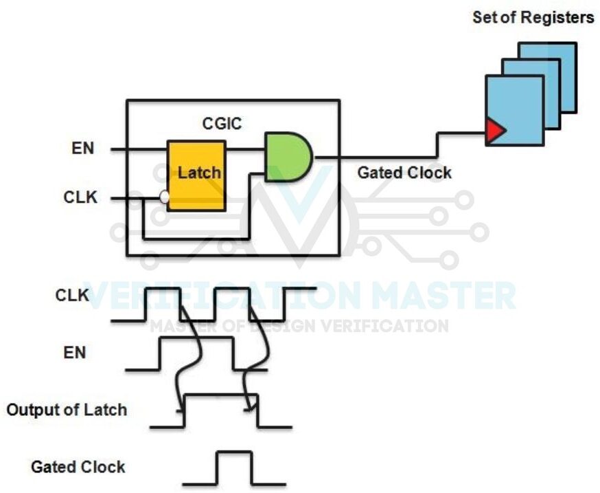
While modern microcontrollers use more sophisticated, glitch-free circuits called Integrated Clock Gating (ICG) cells, the principle remains the same: a software-controllable 'enable' signal controls whether a peripheral receives a clock or not.
2. Microcontroller Architecture for Clock Gating
So, how does this translate from a single gate to a complex System-on-Chip (SoC)? In ARM-based microcontrollers like the STM32 family, this is managed by the Reset and Clock Control (RCC) peripheral.
The RCC acts as a centralized switchboard for all clocks in the MCU. It takes inputs from various oscillators (HSE, HSI, etc.), uses PLLs to generate high-frequency system clocks, and then distributes these clocks to the CPU core, memories, and all the peripherals (UART, SPI, ADC, etc.) via a system of buses.
A typical STM32 clock tree. The RCC distributes clocks from sources like HSE/HSI through PLLs to the main AHB bus, and then through prescalers to the APB1 and APB2 peripheral buses.
Peripherals are grouped onto different buses, like the Advanced High-performance Bus (AHB) for high-speed peripherals (DMA, memory) and the Advanced Peripheral Buses (APB1, APB2) for lower-speed ones (UART, I2C, Timers).
The crucial feature for clock gating is that the RCC has a set of peripheral clock enable registers. Each bit in these registers corresponds to a specific peripheral and acts as the 'enable' signal for its clock gate.
STM32 Clock Configuration Guide
This article provides a very clear explanation of how these enable registers work in STM32 microcontrollers.
Please read the section titled 'Peripheral Clock Gating and Autonomous Mode'. This section is the core of our lesson and directly explains the registers and the mechanism for enabling/disabling peripheral clocks.
3. Implementation in C
As you just read, peripherals are dead—their registers cannot be accessed—until their clock is enabled. This is a common source of bugs for developers new to bare-metal programming. If you try to write to a peripheral register without first enabling its clock in the RCC, your program will likely hang in a HardFault because of an invalid bus access.
The clock enable registers are typically named RCC_AHBxENR and RCC_APBxENR (e.g., RCC_AHB1ENR, RCC_APB2ENR).
Practical Example: Enabling and Disabling a UART
Let's consider a practical scenario. You have a UART peripheral that you only use for occasional debug logging. To save power, you want to disable its clock when it's not in use.
Most vendor HAL (Hardware Abstraction Layer) libraries provide macros to simplify this. For an STM32F4, enabling the clock for USART2 (which is on the APB1 bus) would look like this:
// Using the ST HAL macro to enable the USART2 clock
__HAL_RCC_USART2_CLK_ENABLE();
This macro is simply a wrapper around a direct register write. It expands to something like:
// The underlying register manipulation for enabling USART2 clock
// RCC_APB1ENR_USART2EN is a bitmask for the USART2 enable bit.
RCC->APB1ENR |= RCC_APB1ENR_USART2EN;

// As the article mentioned, it's good practice to have a small delay
// or memory barrier after enabling a clock before register access.
// Reading the register back is a common way to ensure the write has completed.
(void)RCC->APB1ENR;
To disable the clock and reduce power, you simply clear the bit:
// Using the ST HAL macro to disable the USART2 clock
__HAL_RCC_USART2_CLK_DISABLE();

// Which expands to:
RCC->APB1ENR &= ~RCC_APB1ENR_USART2EN;
Driver Implementation Strategy
A robust driver should manage its own clock.
- The
My_UART_Init()function should be the one to enable the clock. - You should provide a
My_UART_DeInit()function that, among other things, disables the clock.
void My_UART_Init(void) {
    // 1. Enable the peripheral clock
    __HAL_RCC_USART2_CLK_ENABLE();
    __HAL_RCC_GPIOA_CLK_ENABLE(); // Also need clock for the GPIO pins

    // 2. Configure GPIO pins for UART TX/RX alternate function
    // ...

    // 3. Configure UART parameters (baud rate, word length, etc.)
    // ...

    // 4. Enable the UART peripheral itself
    USART2->CR1 |= USART_CR1_UE;
}

void My_UART_DeInit(void) {
    // 1. Disable the UART peripheral
    USART2->CR1 &= ~USART_CR1_UE;

    // 2. Disable the peripheral clock to save power
    __HAL_RCC_USART2_CLK_DISABLE();

    // The GPIO clock can also be disabled if no other peripheral
    // on that port is in use.
}
The application layer can then call My_UART_Init() when it needs to log data and My_UART_DeInit() when it's done. This is far more power-efficient than leaving the clock running for the entire uptime of the device.
Test your understanding!
You are debugging a new driver for an SPI peripheral. Your SPI_Init function enables the SPI clock in the RCC, configures all the SPI registers, and then enables the SPI peripheral. However, your code immediately faults on the very first register access (SPI1->CR1 = ...). You have double-checked the peripheral's base address and the register offsets, and they are correct. What is the most likely cause of this fault?
Show answer
The most likely cause is that you enabled the clock for the SPI peripheral but forgot to enable the clock for the GPIO port that the SPI pins (SCK, MISO, MOSI) belong to. Before you can configure a GPIO pin for an alternate function (like SPI), its port's clock must be enabled via its respective RCC_AHBxENR register. Accessing the GPIOx->MODER or GPIOx->AFR registers without the port being clocked would cause a bus fault.
4. Interview Corner: Power Optimization Strategy
An interviewer might ask a high-level question to gauge your architectural thinking: "You're tasked with writing the firmware for a battery-powered sensor that wakes up, takes a measurement, transmits it, and goes back to sleep. Describe your software strategy for minimizing power consumption."
This is your chance to bring together everything from this module. Here's how you could structure your answer:
-
RTOS and Low Power Modes: "I would build the application on an RTOS like FreeRTOS and leverage its tickless idle feature. This allows the system to enter a deep sleep mode (like STM32's STOP mode) for the majority of its life, suppressing the tick interrupt to prevent unnecessary wake-ups."
-
Aggressive Clock Gating (Pre-Sleep): "Before entering STOP mode, in the
configPRE_SLEEP_PROCESSINGhook, I would implement an aggressive clock gating policy. I would disable the clocks to every single peripheral that is not required to wake the system up. This includes the ADC, communication interfaces like SPI/I2C, DMA, and any timers not used for wake-up." -
Active Power Management: "Power savings aren't just for sleep. During the brief active period, I would apply clock gating dynamically. For example, the ADC clock would only be enabled right before a measurement is taken and disabled immediately after. Similarly, the radio's SPI/UART clock would be enabled only during the transmission phase and then shut off."
-
Clock Scaling: "I would also analyze if the CPU needs to run at its maximum frequency. If the processing tasks are not intensive, I could scale down the system clock frequency. Since dynamic power scales with frequency, running at 24 MHz instead of 96 MHz, if possible, provides significant savings. The goal is to run 'just fast enough' to get the job done and get back to sleep."
-
Driver Design: "Finally, all my low-level drivers would be designed with power in mind. Each driver's
initfunction would enable its required clocks, and each would have adeinitfunction that disables those clocks, allowing the application layer to easily power-manage peripherals."
This answer demonstrates a multi-layered approach, from the RTOS level down to individual driver implementation, which is exactly what an experienced embedded engineer is expected to know.
Conclusion
You have now completed the module on Advanced System Optimization. By mastering processor low-power modes, RTOS tickless idle, and now peripheral clock gating, you have the essential tools to design and implement highly power-efficient embedded systems.
Key Takeaways:
- Dynamic power is proportional to clock frequency; stopping a clock (
f=0) eliminates its dynamic power draw. - The RCC peripheral controls clock distribution and provides per-peripheral enable bits in registers like
RCC_AHBxENRandRCC_APBxENR. - A peripheral's clock must be enabled before its registers can be accessed.
- Effective power management involves gating clocks not only before deep sleep but also dynamically during active operation when a peripheral is temporarily idle.
Next Lesson Preview:
We have focused on optimizing the system at a high level. In our next module, Advanced ARM Architectures, we will shift our focus to the processor core itself. We will begin by exploring the features of the ARMv7-A/R architecture, the foundation for the powerful application processors found in complex automotive systems, and introduce concepts like the Memory Management Unit (MMU) and virtual memory.