Recommended resources
The freely available resources this lesson will direct you to.
Hello! Welcome to your next lesson in our "Semiconductor Physics and Transport" module.
In our last lesson, we introduced the powerful concept of effective mass, . We saw that by bundling the complex effects of the periodic crystal potential into this single parameter, we can treat electrons and holes as quasi-classical particles. We derived that is determined by the curvature of the bands and previewed that it would be a crucial ingredient in calculating the density of charge carriers.
Today, we will make good on that promise. Our goal is to calculate the concentration of electrons () and holes () in a semiconductor. We will investigate how these concentrations are determined by temperature and the intentional introduction of impurities, a process known as doping. This is fundamental to designing and understanding any semiconductor device.
We will proceed in four steps:
- Derive the general expressions for and by combining the density of states with the Fermi-Dirac distribution.
- Analyze the special case of an undoped (intrinsic) semiconductor and derive the famous law of mass action.
- Examine how doping creates extrinsic semiconductors where one carrier type dominates.
- Explore the full temperature dependence of carrier concentration, from low-temperature "freeze-out" to the high-temperature "intrinsic" regime.
1. Carrier Concentration from First Principles
The number of electrons per unit volume in the conduction band, , is the integral over all conduction band energies of the density of available states, , multiplied by the probability that each state is occupied, .
Let's break down the two components of the integrand.
The Fermi-Dirac Distribution
As you know from statistical mechanics, the probability that an electronic state of energy is occupied at temperature is given by the Fermi-Dirac distribution:
where is the Fermi level. For most semiconductors under typical operating conditions (non-degenerate), the Fermi level is located within the band gap, several away from the band edges. For electrons in the conduction band, , so . This allows us to use the Boltzmann approximation:
The Density of States
In the previous lesson, we established that near a band minimum, we can approximate the band as parabolic: . The density of states for such a 3D parabolic band is:
Notice the direct dependence on the electron effective mass, .
Performing the Integration
Combining these gives:
This integral can be solved using a change of variables and the definition of the Gamma function. The result is a concise and powerful expression for the electron concentration:
where is the effective density of states in the conduction band:
Physically, represents the total number of effective states per unit volume available to electrons in the conduction band, as if they were all located at the band edge .
A completely analogous derivation for holes in the valence band (using the hole effective mass ) yields:
where is the effective density of states in the valence band.
For a formal walkthrough of this derivation, please refer to the following resource.
Electrons and Holes in Semiconductors
The text 'Electrons and Holes in Semiconductors' provides a clear, step-by-step derivation of the electron and hole concentration equations.
Please read Section 1.7.2, 'Fermi Function', and Section 1.8.1, 'Derivation of n and p from D(E) and f(E)'. This will solidify your understanding of how the density of states and Fermi function combine to give the final expressions for n and p, including the definitions of Nc and Nv.
2. Intrinsic Semiconductors and the Law of Mass Action
An intrinsic semiconductor is perfectly pure, with no dopant atoms. In this case, the only charge carriers are electrons that have been thermally excited from the valence band to the conduction band, leaving holes behind. This process creates electron-hole pairs, so their concentrations must be equal: . This concentration is called the intrinsic carrier concentration, .
A remarkable relationship emerges if we multiply our expressions for and :
Recognizing that (the band gap energy), we get:
The key insight here is that the product is independent of the Fermi level and depends only on temperature and fundamental material properties (, , ). For a given material at a fixed temperature, this product is constant. This is the Law of Mass Action.
Since for an intrinsic material , we can write:
Therefore, the intrinsic carrier concentration is:
The exponential dependence on makes extremely sensitive to both the band gap and temperature. For silicon ( eV) at room temperature (300 K), . For GaAs ( eV), is much lower, around .
Electron & Hole Concentration at Equilibrium: Lecture-10
The following video provides a good summary of deriving intrinsic electron and hole concentrations and explains the mass action law.
Watch the segment from 9:59 to 14:41. This section walks through the derivation of the intrinsic carrier concentration and the law of mass action, np = n_i^2.
3. Extrinsic Semiconductors and Doping
The electrical properties of semiconductors are rarely left to the whims of thermal generation. Instead, they are precisely controlled by doping—the intentional introduction of impurity atoms.
- Donors (): Impurities with more valence electrons than the host atom (e.g., Phosphorus in Silicon). They easily "donate" an electron to the conduction band, becoming a fixed positive ion. This creates an N-type semiconductor.
- Acceptors (): Impurities with fewer valence electrons (e.g., Boron in Silicon). They easily "accept" an electron from the valence band to complete their bonds, creating a mobile hole and becoming a fixed negative ion. This creates a P-type semiconductor.
The master equation governing carrier concentrations in any scenario is charge neutrality: the total positive charge density must equal the total negative charge density.
where and are the concentrations of ionized donors and acceptors.
At room temperature, the ionization energy for common dopants is small compared to , so we can assume complete ionization: and . The equation becomes:
This equation, combined with the law of mass action (), allows us to find and for any doping situation.
Case 1: N-type Semiconductor
Here, . Since electrons are abundant, . Also, is usually negligible compared to the doping level. The neutrality equation simplifies to:
The electron concentration is determined by the net donor concentration. These are the majority carriers. The hole concentration, the minority carriers, is then found from the law of mass action:
Case 2: P-type Semiconductor
Here, . By the same logic, holes are the majority carriers:
And electrons are the minority carriers:
This phenomenon, where acceptors can cancel the effect of donors (and vice-versa), is called dopant compensation.
Test your understanding!
A silicon sample at 300 K is doped with donors and acceptors. For Si at 300 K, . Calculate the electron and hole concentrations.
Show answer
- First, determine the semiconductor type. Since , it is N-type.
- The majority carrier concentration (electrons) is given by the net doping:
- The minority carrier concentration (holes) is found using the law of mass action:
Notice how the presence of majority carriers drastically suppresses the minority carrier population compared to the intrinsic value.
For a more rigorous treatment that doesn't make approximations upfront, we can solve the system of equations directly. Substituting into the charge neutrality equation gives a quadratic equation for . This is particularly relevant for compensated semiconductors or near-intrinsic conditions.
Temperature-dependence of carrier concentration
This video from NPTEL provides an excellent derivation of the quadratic equation for carrier concentration based on the charge neutrality principle, which is essential for understanding compensated semiconductors.
Please watch from 3:22 to 11:30. The instructor carefully sets up the charge neutrality equation and solves it to find the carrier concentration in a semiconductor doped with both donors and acceptors.
4. Temperature Dependence of Carrier Concentration
Plotting the logarithm of the majority carrier concentration (e.g., for an N-type material) versus inverse temperature () reveals three distinct regimes. This is a classic plot you would generate from a Hall effect experiment.
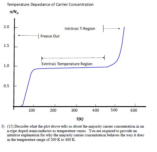
-
Low Temperature: Freeze-out Regime
At very low temperatures, the thermal energy is insufficient to ionize all the donor atoms. The electrons are "frozen" onto the donor sites. As temperature increases, more donors are ionized, and the carrier concentration rises exponentially. The slope of the vs plot in this region is proportional to the donor ionization energy, . -
Intermediate Temperature: Extrinsic (Exhaustion) Regime
In this range (which includes room temperature for Si), thermal energy is high enough to ionize essentially all dopant atoms () but not high enough to create a significant number of electron-hole pairs across the band gap (). The carrier concentration is constant and determined by the doping level. This is the region where most semiconductor devices are designed to operate, as it provides stable and predictable behavior. -
High Temperature: Intrinsic Regime
At very high temperatures, thermal energy becomes so large that electrons are excited across the entire band gap in huge numbers. The intrinsic concentration grows exponentially and eventually overwhelms the dopant concentration (). The semiconductor loses its "extrinsic" character and behaves as if it were intrinsic, with . The slope of the plot in this regime is proportional to .
This temperature dependence has significant implications. For instance, the transition to the intrinsic regime sets an upper limit on the operating temperature of a device. Materials with wider band gaps (like GaN or SiC) have a much smaller at a given temperature, so they can operate at higher temperatures before becoming intrinsic. This is why they are used in high-power and high-temperature electronics.
Temperature-dependence of carrier concentration
To see a detailed discussion of these three regimes, watch the following segment.
Watch from 17:31 to 28:34. This part of the lecture provides a clear explanation of the freeze-out, extrinsic, and intrinsic regions and discusses the importance of wide-bandgap materials for high-temperature applications.
For the Mathematically Curious: An Exact Solution
The standard approach simplifies the charge neutrality equation for different regimes. However, it's possible to find an exact analytical solution that is valid across all temperatures. By considering the partial ionization of dopants (i.e., not assuming ), one can derive a cubic equation for the carrier concentration (or a related variable). Solving this equation gives the carrier concentration without any approximation. Given your background, you might find this more rigorous approach interesting. The paper "An Exact Analysis for Freeze-out and Exhaustion in Single Impurity Semiconductors" (resource LINK) by Pieper and Michael details this method. It's a nice example of applying formal mathematical techniques to obtain a more complete physical picture.
Conclusion
In this lesson, we have built a quantitative model for determining the concentration of charge carriers in a semiconductor. This is a cornerstone of semiconductor physics, bridging the gap between the abstract band structure and the tangible electrical properties of a material.
Key Takeaways:
- Carrier concentrations are calculated by integrating the product of the density of states and the Fermi-Dirac occupation function .
- For non-degenerate semiconductors, this leads to the relations and , where and depend on temperature and the effective masses.
- The Law of Mass Action states that in thermal equilibrium, the product is a constant for a given material and temperature, regardless of doping.
- Doping allows for precise control of majority carriers. In the extrinsic regime, the majority carrier concentration is approximately equal to the net dopant concentration (e.g., ).
- The temperature dependence of carriers defines three critical regions: freeze-out, extrinsic, and intrinsic, which dictate the operational limits of a semiconductor device.
Preview of Next Lesson:
We now understand how to populate a semiconductor with a desired number of electrons and holes. What happens when we join a P-type region with an N-type region? In the next lesson, we will analyze the formation of a p-n junction. We will solve the Poisson equation to understand how charge carrier diffusion and drift lead to the creation of a depletion region and a built-in potential, which are the essential features of diodes, transistors, and many other semiconductor devices.