Recommended resources
The freely available resources this lesson will direct you to.
Hello! Last lesson established the heat generated by each component and where that heat originates. The next question is spatial: how does energy leave a component’s hot region and reach the surroundings? This lesson builds a heat-flow map for a PCB inside a sealed enclosure. You will use that map to recognize the important solid, air, and surface paths before calculating temperatures or building a CFD model.
Begin at the junction, not at the enclosure wall
For a semiconductor IC, the junction is the internal region where its assigned power loss becomes heat. The surrounding package is not necessarily at the same temperature. Heat must travel through package materials before it can enter the PCB, the enclosed air, or a deliberately attached heat spreader.
Three mechanisms describe the journey:
- Conduction transfers heat through solids, such as a die attach, solder joint, copper plane, mounting bracket, or enclosure wall.
- Convection transfers heat between a surface and moving air. Inside a sealed box, that air may move by buoyancy even though none enters or leaves.
- Radiation transfers energy between surfaces. It can connect a component or PCB surface directly to an interior enclosure surface without first heating the air.
Read the short explanation of these mechanisms in ROHM’s Basics of Thermal Resistance and Heat Dissipation. Keep the physical mechanisms in mind; you do not need to calculate a thermal resistance yet.
[PDF] Basics of Thermal Resistance and Heat Dissipation
ROHM’s application note distinguishes the three ways heat can cross the regions of an electronics assembly. Read it to give each segment of your eventual path diagram the right physical label.
On printed p. 2, find “Heat transfer and heat dissipation path,” then its subsection “Three forms of heat transfer.” Read the three descriptions, stopping after the explanation that radiation needs no intervening medium. Focus on where a solid, moving fluid, or pair of surfaces is required; do not assume one mechanism must always dominate the others.
A useful rule for the drawing is to mark physical regions and interfaces, not just temperatures. “Junction to ambient” names the endpoints, but conceals nearly every engineering decision between them.
Draw the component and PCB paths first
The first image shows a packaged semiconductor mounted on a PCB. Its red marks indicate several routes out of the hot die region: through the package and leads, and into the board. The image ends at an exposed PCB test environment; your sealed-enclosure drawing must continue beyond the PCB.
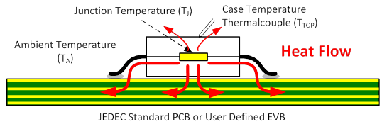
For a package with an exposed thermal pad, one potentially strong route runs through the die attach and metal pad, across solder, and into PCB copper. Copper planes spread heat across the board; thermal vias can connect a landing pad to buried planes or the opposite board face. A different package may send more heat through its leads or upper surface. Draw the paths the actual package provides, rather than assuming every IC is cooled primarily through its top.
The following reading supplies the package and board detail behind those marks.
Using Thermal Calculation Tools for Analog Components
In Using Thermal Calculation Tools for Analog Components, Texas Instruments traces heat through an exposed-pad package and explains why the PCB landing pad, copper spreading plane, and vias matter. Use this as a concrete package example, not as a claim that all packages have the same dominant path.
In Section 2, “Exposed Pad Packages,” locate Figure 2, “Exposed Pad Package Thermal Path” (around printed pp. 2–3). Read the package description; identify each material between the die and board. Then, on printed p. 3 in Section 3, “PCB Design,” use Figure 3 to orient yourself and read the board-path discussion, including items “a. Landing pad,” “b. Spreading plane,” and “c. Vias.” Look for the difference between crossing the PCB stack and spreading heat along its copper.
At this point, a sketch should have branches, not a single uninterrupted line. From the junction, some heat can reach the board through a pad, solder, and copper; some can reach it through leads; and some can reach the package exterior. A branch becomes important only if its package construction, contacts, area, and subsequent route offer an effective way to remove heat. You cannot determine the fractions from an image alone.
Continue every branch through the sealed enclosure
Enclose the PCB sketch within a box representing the enclosure wall. Label the air space internal air and the region outside external surroundings. This immediately prevents a common mistake: drawing an air path that exits through a wall that is meant to be sealed.
From the board and package, look for three kinds of onward connection:
| Connection to mark on the sketch | What physically carries heat |
|---|---|
| Exposed package or PCB surface to interior wall | Heat crosses into internal air; buoyant air circulation transports it around the cavity; it crosses from air into the cooler wall. |
| Exposed package or PCB surface to interior wall | Radiation exchanges energy directly between those surfaces. |
| PCB or component to enclosure wall through a mount | Heat conducts through contacting solids, such as a fastener, bracket, heat spreader, or thermal interface. Mark this route only if that contact exists. |
The first two entries have the same broad endpoints but are different physical paths. Radiation goes from surface to surface, not “through the air.” Internal convection involves heat exchange at solid–air surfaces and circulation of the enclosed air. They can operate simultaneously. A narrow, obstructed gap can restrict air motion; it does not automatically eliminate heat transfer across the gap.
The video Better Electronics Enclosure Design with Thermal Simulation, from SimScale, shows both a simplified sealed-PCB geometry and a calculated internal-air circulation pattern. Watch for the distinction between where heat is generated and how the trapped air redistributes it.
Better Electronics Enclosure Design with Thermal Simulation
Watch the enclosure example in Better Electronics Enclosure Design with Thermal Simulation (SimScale). Its useful feature here is the visible relationship among the chips, board, air cavity, and casing—not the particular simulation software or reported temperatures.
Watch the enclosure geometry to locate the three heat-generating chips and their surrounding sealed case. Then watch the air circulation: observe warmed air rising near the chips, transferring heat near the casing, and circulating back within the cavity. Treat those streamlines as an internal transport route, not as air escaping to the room.
The second image makes the same distinction explicit. The large loops stay inside the enclosure; the marks outside represent heat leaving its external surfaces.
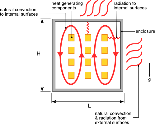
There is one indispensable final connection. Heat conducted into the enclosure wall reaches its outer surface. From there, the wall can transfer heat by convection to external air and by radiation to surrounding surfaces. External air temperature and the temperatures of surrounding surfaces need not be identical. If the enclosure is also attached to a larger structure, that contact may provide an additional conductive exit route; do not draw one unless the installation includes it.
This is why sealed does not mean insulated. The wall prevents bulk exchange of inside and outside air. It does not prevent conduction through itself or heat transfer from its exterior.
Assemble a junction-to-ambient path map
You can now draw a useful diagram without guessing heat-transfer coefficients. Use a cross-section of the intended assembly, then annotate it in this order:
- Mark sources. Put each heat-generating region inside the component that actually dissipates the watts. In last lesson’s example, the converter IC, inductor, and two loads were four separate sources, not one heat source at the converter.
- Mark real solid connections. Include the relevant package layers, solder, PCB copper, vias, board supports, and any deliberate contact with the enclosure. Leave out imagined contacts across air gaps.
- Mark exposed surfaces. Identify package and board faces that see internal air or other interior surfaces. Indicate both air-mediated and radiative routes where they may matter.
- Finish at the correct surroundings. Continue through the enclosure wall to its exterior, then label external air and surrounding surfaces. Show a separate mounting-contact exit if the enclosure has one.
For a typical board-mounted, exposed-pad IC, the board route on that drawing includes the junction, die attach, pad and solder, PCB copper or vias, and then whichever board-to-wall connections actually exist: air exchange, radiation, or a solid mount. Its package-exterior route includes the junction, package material, and the exposed package surface before connecting through internal air or radiation to the wall. Both routes share the enclosure wall and its exterior heat rejection as their eventual way out.
“Dominant” is a judgment about this complete route. A highly conductive PCB copper plane may spread heat effectively, yet a poor board-to-enclosure connection can still limit that branch. Conversely, a modest package-to-board path might become valuable if the board has a well-coupled metal mounting point. A good local segment does not guarantee a good junction-to-ambient path. Until you have dimensions, material information, and temperatures—or a simulation or measurement—mark uncertain branches as possible, not proven dominant.
For a first Fluent model, this map will later tell you which regions deserve separate solid bodies, where an internal-air region is needed, and which surfaces meet one another. It does not yet determine the mesh, the flow model, or the boundary-condition values. Those decisions come after the physical paths are clear.
Closing perspective
A defensible heat-flow drawing starts at each component’s actual heat-generating region and ends outside the sealed enclosure. It distinguishes conduction through packages, PCB features, contacts, and wall; convection involving trapped internal air; radiation between interior surfaces; and heat rejection from the exterior to its surroundings. Most importantly, it preserves parallel paths without inventing a solid contact or an opening for air.
In the next lesson, you will place a steady-state energy balance around the enclosure. That balance will check the whole drawing: heat entering its thermal paths must ultimately be accounted for at the enclosure’s exits.