Recommended resources
The freely available resources this lesson will direct you to.
Hello! Welcome back to our course on Radioelectronics.
In our last lesson, we explored crystal oscillators and saw how they provide an exceptionally stable frequency reference. However, a single, fixed frequency is often not enough. Modern communication systems require the ability to generate a wide range of frequencies for tuning across different channels, all while maintaining the stability of that original crystal reference.
Today, we will study the circuit that accomplishes this: the Phase-Locked Loop (PLL). This lesson addresses the learning outcome: The Phase-Locked Loop (PLL): Architecture and Fundamental Operation. We will deconstruct the PLL into its functional blocks and understand how it operates as a feedback control system to synthesize stable, variable frequencies. This concept is a cornerstone of modern radio frequency (RF) engineering and digital electronics.
1. The PLL as a Frequency Synthesizer
At its core, a Phase-Locked Loop is a negative feedback system designed to synchronize a tunable oscillator with a reference signal. It continuously compares the phase of its output signal (after division) to the phase of a stable reference signal (from a crystal oscillator). It then generates an error signal that adjusts the oscillator's frequency until the phase difference is zero, achieving a "locked" state.
When locked, the output frequency is an exact multiple of the reference frequency, inheriting its stability.
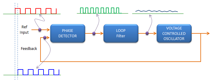
The main components, as shown in the diagram, are:
- Phase Frequency Detector (PFD): The error detector of the system.
- Loop Filter (LF): A low-pass filter that integrates the error signal.
- Voltage-Controlled Oscillator (VCO): A tunable oscillator whose frequency is controlled by a DC voltage.
- Feedback Divider (
/N): A digital counter that divides the VCO output frequency before it's fed back to the PFD.
The fundamental relationship in a locked PLL is:
By changing the division ratio N, we can generate a range of output frequencies, all derived from a single, stable f_{ref}.
To begin, let's get a formal introduction to this architecture.
MT-086: Fundamentals of Phase Locked Loops (PLLs)
This document, 'Fundamentals of Phase Locked Loops (PLLs)' from Analog Devices, provides a clear introduction to the PLL as a negative feedback system. It establishes the core components and the fundamental operating principle.
Please read the first section, 'FUNDAMENTAL PHASE LOCKED LOOP ARCHITECTURE', up to the heading 'PHASE FREQUENCY DETECTOR (PFD)'. Focus on how the PLL is modeled as a standard negative feedback control system and the role of each block in achieving frequency and phase lock.
2. A Closer Look at the Components
Let's examine how each block contributes to the PLL's operation.
a) The Phase Frequency Detector (PFD) and Charge Pump
The PFD is the heart of the feedback loop. It compares the rising edges of the reference signal (f_ref) and the feedback signal (f_out / N). Its job is to produce an output that represents the frequency and phase difference between these two inputs.
A common implementation uses two D-type flip-flops and a delay element.
- If the reference frequency leads the feedback frequency, the PFD outputs a series of "UP" pulses.
- If the reference frequency lags, it outputs "DOWN" pulses.
- The width of these pulses is proportional to the phase difference.
These UP/DOWN pulses drive a charge pump, which is a switchable current source. It injects or removes a small amount of charge from the loop filter capacitor during each pulse, effectively converting the time-domain phase error into a current.
A critical detail in PFD design is avoiding the "dead zone," where for very small phase errors, the PFD might not produce any output, causing the VCO to drift. An "anti-backlash" pulse is intentionally generated even when in lock to prevent this.
The following reading provides an excellent, detailed explanation of the PFD's operation.
MT-086: Fundamentals of Phase Locked Loops (PLLs)
This section of the MT-086 tutorial details the internal workings of a typical PFD, including the flip-flop logic and the charge pump output. It clearly illustrates how the detector responds to frequency and phase differences.
Read the section titled 'PHASE FREQUENCY DETECTOR (PFD)'. Pay close attention to Figure 2 and the accompanying text, which explain the PFD's response when out of lock, close to lock, and fully locked. Note the discussion of the 'dead zone' and the anti-backlash pulse.
b) The Loop Filter (LF)
The loop filter is typically a simple low-pass RC filter. Its primary role is to integrate the current pulses from the charge pump, converting them into a stable DC voltage, often called the tuning voltage (V_tune).
This filtering action is crucial for two reasons:
- Smoothing: It creates the smooth DC voltage needed to control the VCO. Without it, the VCO would be modulated by the individual UP/DOWN pulses, resulting in a noisy output.
- Stability: The loop filter's characteristics (specifically its bandwidth) are the primary determinant of the PLL's dynamic behavior. It controls how quickly the loop can lock onto a new frequency (lock time) and ensures the stability of the feedback system. A narrow filter provides better filtering of unwanted noise but results in a slower lock time.
c) The Voltage-Controlled Oscillator (VCO)
The VCO is an oscillator circuit (like the LC oscillators we've studied) that includes a voltage-variable capacitor, or varactor diode. The V_tune from the loop filter is applied to this varactor, changing its capacitance and thus tuning the oscillator's resonant frequency.
The key trade-off in VCO design is between phase noise, frequency tuning range, and power consumption. A high-Q resonant circuit produces low phase noise but has a narrow tuning range. Conversely, a VCO that can tune over a wide frequency range (an "octave," for example) will inherently have higher phase noise.
Phase-Locked Loop (PLL) Fundamentals
This article from Analog Dialogue provides a concise overview of the VCO's role and the design trade-offs involved.
Read the section titled 'Voltage Controlled Oscillators (VCOs)'. Focus on understanding the fundamental trade-off between phase noise, frequency coverage, and power.
d) The Feedback Divider (N)
This is a programmable digital counter that divides the VCO's high output frequency f_out by an integer N. The result, f_out / N, is the signal fed back to the PFD. This block is what makes the PLL a frequency synthesizer. By changing the integer N, you command the loop to lock to a new output frequency, N × f_ref.
3. Integer-N Synthesis: Putting It All Together
The architecture we've described is known as an Integer-N PLL. The output frequency can only be an integer multiple of the reference frequency.
Let's consider an example:
- Reference: A stable 10 MHz crystal oscillator (
f_ref = 10 MHz). - Goal: Generate a 900 MHz signal for a radio transmitter.
- Action: Program the feedback divider with
N = 90.
The PLL will operate as follows:
- Initially, the VCO frequency is arbitrary. The PFD compares 10 MHz with
f_out / 90. - The PFD and charge pump generate an error signal that pushes
V_tuneup or down. - The VCO frequency changes in response to
V_tune. - This process continues until the feedback signal
f_out / 90is exactly 10 MHz and phase-locked to the reference. At this point,f_outis precisely 900 MHz.
A key limitation arises from this relationship. The smallest frequency step you can make (the channel spacing) is equal to f_ref. If you need 25 kHz channel spacing, you would need f_ref = 25 kHz. To generate 900 MHz, N would have to be 900,000 / 25 = 36,000.
This presents a major problem: noise within the PLL loop (from the PFD and other components) is amplified by a factor of 20log(N). A large N value leads to significantly higher phase noise on the output, which is highly undesirable. This creates a fundamental trade-off in Integer-N PLLs between fine frequency resolution (low f_ref) and low phase noise (low N).
The following readings discuss this architecture and its performance characteristics.
Phase-Locked Loop (PLL) Fundamentals
These sections discuss the Integer-N architecture, the use of prescalers for high-frequency operation, and the trade-offs involved.
First, read the section 'High Frequency Integer-N Architecture'. Then, read 'Integer-N and Fractional-N Divider'. Focus on the Integer-N parts. Note the discussion of phase noise being increased by 20log(N). You can skim the Fractional-N part, as we will not cover it in detail today.
MT-086: Fundamentals of Phase Locked Loops (PLLs)
For a deeper look at the practical implementation of the N-divider, this reading explains why a prescaler is necessary for high-frequency signals and how a dual-modulus prescaler works.
Read the section titled 'PRESCALERS'. This explains the motivation for using a prescaler and the clever operation of the dual-modulus prescaler, which allows for high-speed division without sacrificing resolution. Given your background, the logic behind the N = BP + A equation should be straightforward.
Conclusion
In this lesson, we have dissected the Phase-Locked Loop and understood its operation as a versatile frequency synthesizer.
Key Takeaways:
- A PLL is a negative feedback control system that locks the phase and frequency of a VCO to a stable reference.
- The core components are the Phase Frequency Detector (PFD), Loop Filter, Voltage-Controlled Oscillator (VCO), and a feedback divider (N).
- The fundamental relationship in a locked Integer-N PLL is
f_out = N × f_ref, allowing the synthesis of multiple stable frequencies from a single reference. - The PFD acts as an error detector, the loop filter integrates the error into a control voltage, and the VCO generates the output frequency.
- There is a critical trade-off in Integer-N synthesizers between frequency resolution (channel spacing) and phase noise, as noise is amplified by
20log(N).
The PLL is a foundational building block in almost every modern radio. The ability to generate precise, stable, and agile local oscillator (LO) signals is what enables transmitters and receivers to tune to different channels.
In our next module, we will begin our study of Analog Communication Systems. We will see precisely how the stable LO signals generated by PLLs are used in the process of modulation to impress information onto a high-frequency carrier wave for transmission.