Recommended resources
The freely available resources this lesson will direct you to.
- A Deep Dive into NVIDIA Blackwell with SemiAnalysis' Dylan Patelwww.youtube.com
- Multi-GPU Communication Libraries for Scaling HPC and AI Workloads | NVIDIA GTC 2025www.youtube.com
- Multi-GPU Communication: NVLink vs PCIe, NCCL, and Distributed ...www.abhik.ai
- [PDF] Evaluation of On-Node GPU Interconnects for Training Deep Neural ...mediatum.ub.tum.de
Introduction
Welcome to the first lesson in our new module, "Multi-GPU Communication: Interconnects and Collectives." In our previous module, we focused on optimizing machine learning workloads for a single GPU. We explored techniques like operator fusion and mixed-precision training, which are crucial for extracting maximum performance from one device. However, the sheer scale of modern AI models, particularly in the large language model (LLM) space, often exceeds the memory and computational capacity of any single GPU.
This brings us to the next frontier: scaling out across multiple GPUs. Doing so introduces a new critical bottleneck: communication. The efficiency of a multi-GPU system is fundamentally limited by how quickly and effectively the GPUs can exchange data.
In this lesson, we will examine the physical hardware layer that enables this communication within a single server or node. Our goal is to compare intra-node interconnects like PCIe and NVLink/NVSwitch in terms of their bandwidth, latency, and topology.
We will explore:
- PCI Express (PCIe): The universal, standard interconnect.
- NVLink and NVSwitch: NVIDIA's proprietary, high-performance interconnect fabric.
- A quantitative comparison of their performance characteristics and architectural trade-offs.
Understanding these hardware foundations is the first and most critical step in designing and optimizing large-scale AI training systems.
1. The Need for Inter-GPU Communication
Before diving into the hardware, let's briefly establish why GPUs need to talk to each other. When you distribute a training job across multiple GPUs, they can no longer work in isolation. Depending on the parallelization strategy, they need to exchange information constantly:
- In Data Parallelism, each GPU processes a different slice of the input data. After computing gradients, they must all communicate to average their results before updating the model weights.
- In Model Parallelism, the model itself is split across GPUs. To process even a single data sample, GPUs must pass activations forward and gradients backward between each other.
This constant data exchange—gradients, activations, weights—makes the performance of the interconnect paramount.
2. PCI Express (PCIe): The Universal Standard
Peripheral Component Interconnect Express (PCIe) is the default high-speed interface used to connect components like graphics cards, storage drives, and network cards to a computer's motherboard.
Topology
A PCIe bus uses a point-to-point, tree-like topology. Each device gets a dedicated serial link to a central switch or the CPU's root complex. The links are composed of one or more "lanes." A modern GPU typically uses a 16-lane (x16) connection.
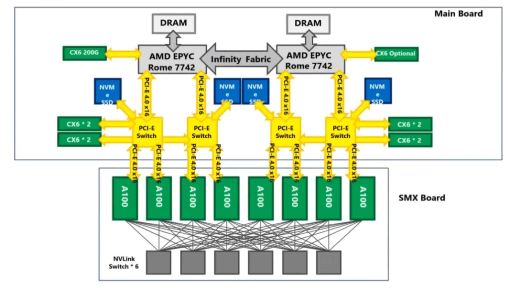
In a multi-GPU system using only PCIe, GPUs do not communicate directly. For GPU A to send data to GPU B, the data must travel "up" the PCIe bus to a common switch or the CPU, and then "down" to the target GPU. This indirect path introduces latency and can become a significant bottleneck, as the root switch's bandwidth is shared among all connected devices.
Bandwidth
PCIe bandwidth scales with the number of lanes and the generation of the standard. Each new generation roughly doubles the bandwidth per lane.
Multi-GPU Communication: PCIe: The Universal Standard
To get a clear overview of PCIe and its performance characteristics, please review the following resource.
Read the section titled 'PCIe: The Universal Standard'. Pay close attention to the table showing the bandwidth for different PCIe generations (Gen3, Gen4, Gen5).
As you saw, a PCIe Gen5 x16 link provides 64 GB/s of unidirectional bandwidth (128 GB/s bidirectional). While substantial, this can be quickly saturated by the communication demands of large-scale model training.
- Pros: Universal, compatible with all CPUs and GPUs.
- Cons: Lower bandwidth than specialized interconnects, communication path often involves the CPU or a shared switch, creating potential bottlenecks.
3. NVLink and NVSwitch: The High-Speed, Direct Lane
To overcome the limitations of PCIe for high-performance computing (HPC) and AI workloads, NVIDIA developed NVLink, a proprietary, high-bandwidth, direct GPU-to-GPU interconnect.
Topology and Bandwidth
Unlike PCIe, NVLink provides a direct point-to-point connection between GPUs, bypassing the CPU and PCIe bus entirely. This dramatically increases bandwidth and reduces latency.
Over successive generations, the topology has evolved:
- Direct Links: Early implementations (e.g., Pascal P100 GPUs) used a fixed number of NVLink connections per GPU to create a static
hybrid cube-meshtopology, directly connecting each GPU to a few of its peers. - Switched Fabric (NVSwitch): Modern systems (e.g., A100, H100) use a dedicated chip called NVSwitch. Multiple NVSwitches create a full, non-blocking crossbar fabric. This allows any GPU in the server to communicate with any other GPU at the full NVLink bandwidth simultaneously. This is a crucial evolution, as it provides all-to-all communication without contention, achieving full bisection bandwidth.
The following resource and image provide an excellent comparison.
Multi-GPU Communication: NVLink and NVSwitch
Now, let's explore NVLink and NVSwitch in more detail to contrast them with PCIe.
Read the sections 'NVLink: NVIDIA's High-Speed Lane' and 'NVSwitch: Full-Mesh Connectivity'. Note the generational improvements in bandwidth and how NVSwitch solves the topology problem.

- Pros: Extremely high bandwidth and low latency, direct GPU-to-GPU communication path, full bisection bandwidth with NVSwitch.
- Cons: Proprietary to NVIDIA GPUs, higher system cost.
4. A Deeper Dive: Microbenchmark Performance
Theoretical specifications are one thing; real-world performance is another. Since you have a strong academic background, you may appreciate looking at experimental data. The following resource is a thesis that conducted microbenchmarks to measure the effective bandwidth of PCIe and NVLink in DGX systems.
Evaluation of On-Node GPU Interconnects for Training Deep Neural Networks
To see how these theoretical differences play out in practice, we'll look at some experimental results from a paper that performed microbenchmarks on real multi-GPU systems. This provides concrete data on bandwidth and latency.
Please read the following sections: Chapter 4, Section 4.1 ('Microbenchmarks'); and in Chapter 5, read Sections 5.1, 5.1.1, 5.1.2, and 5.3 ('Discussion of Results'). Focus on Figures 5.2 and 5.6, which show the measured bandwidths, and the summary in Section 5.3 that contrasts the practical performance of NVLink vs. PCIe.
Key Experimental Insight
A crucial takeaway from that paper is that NVLink not only has a higher nominal (theoretical) bandwidth but also achieves a much higher percentage of it in practice. The microbenchmarks showed NVLink reaching 80-90%+ of its theoretical bandwidth, while PCIe connections often topped out at 60-70%. This is because NVLink's protocol is leaner and optimized for GPU-to-GPU traffic, whereas PCIe is a more general-purpose protocol with higher overhead. This widens the effective performance gap between the two even further.
5. The System-Level Impact: Scaling the NVLink Domain
The choice and evolution of these interconnects have profound implications for AI system design. As models grow, the "NVLink domain"—the set of GPUs fully interconnected by the NVSwitch fabric—becomes a fundamental building block of a datacenter. Expanding this domain is a key architectural driver for enabling next-generation AI.
To see where this is heading, the following clip discusses the NVIDIA Blackwell architecture. Note how the expansion of the NVLink domain from 8 GPUs (in the Hopper generation) to 72 GPUs is presented as a major architectural innovation.
A Deep Dive into NVIDIA Blackwell with SemiAnalysis' Dylan Patel
The evolution of these interconnects has profound implications for system architecture. This clip discussing the NVIDIA Blackwell architecture highlights how expanding the NVLink domain is a major driver of performance and a significant system design challenge.
Watch the segment from 10:24 to 13:00. Pay attention to the discussion of how the NVLink domain has expanded from 8 GPUs to 72 GPUs and why this is a significant system architecture change that enables new training and inference techniques.
As the video illustrates, creating a larger, tightly-coupled communication domain allows for more sophisticated parallelism strategies, but also introduces immense system design challenges related to power, cooling, and reliability. This is a core trade-off in modern AI system design.
Conclusion
In this lesson, we dissected the foundational hardware for intra-node GPU communication. We established the clear hierarchy between the universal PCIe standard and the specialized, high-performance NVLink/NVSwitch fabric.
Key Takeaways:
- Topology: PCIe uses a tree-like topology where GPU-to-GPU communication often traverses a CPU or a shared switch. NVLink provides direct GPU-to-GPU links, and NVSwitch creates a full crossbar fabric for all-to-all communication.
- Bandwidth: NVLink offers significantly higher bandwidth than PCIe. The latest generation of NVLink provides over 7 times the bidirectional bandwidth of the latest PCIe generation (1800 GB/s vs. 256 GB/s).
- Latency: Both have low latencies on the microsecond scale, but NVLink's direct path gives it an edge.
- System Impact: The choice of interconnect is a defining architectural decision. High-performance systems rely on NVLink and NVSwitch to create large, high-bandwidth communication domains, which are essential for training state-of-the-art models efficiently.
Preview of the Next Lesson:
Now that we understand how GPUs talk to each other inside a single machine, our next lesson will address how to scale beyond the node. We will explore inter-node technologies like InfiniBand and RDMA, which are critical for building large GPU clusters capable of training foundation models.