Recommended resources
The freely available resources this lesson will direct you to.
Hello! Welcome to our final lesson in the module on Electronic Structure and Band Theory.
In our last session, we classified materials into metals, semiconductors, and insulators based on whether their Fermi level lies within a continuous band or inside a band gap. We learned that the modest band gap in semiconductors allows for thermal excitation of charge carriers, making their conductivity highly dependent on temperature.
Today, we will refine this picture by investigating the momentum-space structure of the band gap. You'll learn to distinguish between direct and indirect bandgaps. This distinction is not just a theoretical detail; it is the single most important factor governing how a semiconductor interacts with light. Understanding this will provide a solid foundation for your interest in the optical properties of solids and directly relates to your experimental work in spectroscopy.
Our goal is to contrast the origins of these two types of bandgaps and explore their profound consequences for light absorption and emission.
1. The Rules of the Game: Energy and Momentum Conservation
When a photon strikes a semiconductor, it can excite an electron from the filled valence band (state ) to the empty conduction band (state ). This process, like all physical interactions, must obey fundamental conservation laws.
-
Energy Conservation: The final energy of the electron must equal its initial energy plus the energy of the absorbed photon.
Here, and are the initial and final crystal momenta of the electron.
-
Momentum Conservation: The final crystal momentum of the electron must equal its initial crystal momentum plus the momentum of the absorbed photon.
A crucial insight comes from comparing the photon's momentum to the scale of the Brillouin zone. A photon corresponding to visible light with energy eV has a wavevector . The edge of a typical Brillouin zone is at a wavevector of , where nm is the lattice constant, giving a scale of .
The photon's momentum is a tiny fraction () of the Brillouin zone's size. Therefore, for electronic transitions, we can make the excellent approximation that the photon provides energy but negligible momentum. The momentum conservation rule simplifies to:
This is the crystal momentum selection rule for optical transitions. It means that on an band structure diagram, an electron absorbing a photon makes a vertical transition.
Optical Transitions in Semiconductors
The following notes from a Cornell course, 'Optical Transitions in Semiconductors', provide a more formal derivation of this selection rule using the framework of time-dependent perturbation theory.
Please read the sections titled 'Optical Transitions in Solids: Energy and Momentum Conservation', 'Optical Interband Transitions in Solids', 'Optical Matrix Element', and 'Crystal Momentum Selection Rule'. Given your QFT I background, you should find the application of Fermi's Golden Rule familiar. The key takeaway is the derivation showing why optical transitions are considered 'vertical' in k-space (k_f \approx k_i).
This "vertical transition" rule is the origin of the distinction between direct and indirect bandgaps.
2. Direct Bandgap Semiconductors
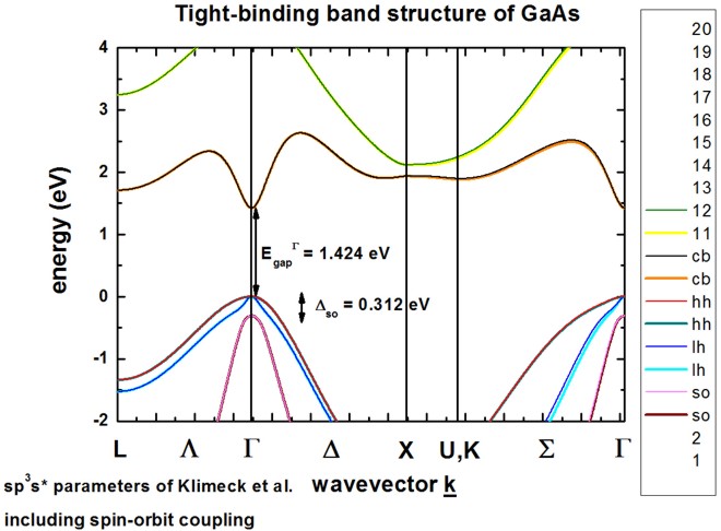
A semiconductor has a direct bandgap if the valence band maximum (VBM) and the conduction band minimum (CBM) occur at the same point in the Brillouin zone. This is most often at the high-symmetry point ().
Optical Consequences of a Direct Gap
- Absorption: An electron at the VBM can directly absorb a photon with energy and jump vertically to the CBM. This is a highly efficient, first-order process involving only the electron and the photon. As a result, direct-gap materials have a strong absorption coefficient () that rises sharply once the photon energy exceeds the band gap.
- Emission: An electron at the CBM can relax back down to the VBM and emit a photon of energy . This radiative recombination is also a vertical, momentum-conserving process, making it fast and efficient. This is why direct-gap semiconductors like GaAs and GaN are the materials of choice for light-emitting diodes (LEDs) and laser diodes.
The absorption coefficient for a direct-gap material follows a characteristic energy dependence near the band edge:
This square-root dependence arises from the joint density of states for parabolic bands in 3D.
The lecture notes 'Optical Properties of Solids' by R.A. Taylor provide a concise explanation of direct transitions and the resulting absorption properties.
Read the subsections titled 'Conditions for direct interband transitions' and 'Dependence of transition probability on photon energy'. Focus on how the three conditions (wavevector, parity, energy) lead to the formula for the absorption coefficient. Note the example plot for GaAs, which clearly shows the sharp absorption edge.
3. Indirect Bandgap Semiconductors
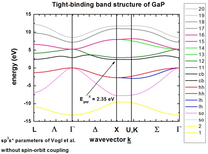
A semiconductor has an indirect bandgap if the VBM and CBM occur at different points in the Brillouin zone. Silicon (Si), for example, has its VBM at the point but its CBM is about 85% of the way to the X point.
Optical Consequences of an Indirect Gap
-
Absorption: For an electron to be excited across the minimum band gap , it must change both its energy and its momentum. Since the photon cannot provide the required momentum change (), the crystal must participate by either absorbing or emitting a lattice vibration quantum—a phonon.
A phonon with wavevector carries momentum and energy . The conservation laws for a phonon-assisted transition are:
- Energy:
- Momentum:
Because this process involves three "particles" (electron, photon, phonon), it is a second-order quantum process. Such processes have a much lower probability than first-order direct transitions. Consequently, the absorption of light near the indirect band edge is significantly weaker.
-
Emission: Radiative recombination is similarly inefficient. An electron at the CBM and a hole at the VBM are much more likely to recombine non-radiatively by emitting a series of phonons, dissipating their energy as heat rather than light. This is why silicon is an exceptionally poor light emitter.
The absorption coefficient for an indirect gap is not only weaker but also has a different energy dependence:
The two terms correspond to processes involving phonon absorption or emission, which become possible at different threshold photon energies.
Let's return to the notes by R.A. Taylor to see how indirect transitions are described.
Read the subsection 'Indirect interband transitions'. Pay close attention to the role of the phonon wavevector \mathbf{q} in conserving momentum and why this makes the process second-order and much weaker. (You can ignore the discussion on excitons for now; we'll cover them in a later module).
4. Summary and Experimental Signatures
The distinction between direct and indirect bandgaps is fundamental to the application of semiconductors in optoelectronic devices.
| Feature | Direct Bandgap | Indirect Bandgap |
|---|---|---|
| VBM/CBM Alignment | Same | Different |
| Momentum Conservation | Photon only () | Photon + Phonon () |
| Process Order | 1st order (efficient) | 2nd order (inefficient) |
| Absorption Strength | Strong ( cm) | Weak ( cm) |
| Absorption Edge | ||
| Radiative Recombination | Efficient | Inefficient |
| Typical Applications | LEDs, Lasers, Modulators | Transistors, Solar Cells (absorption is sufficient) |
Your experience with photoluminescence (PL) spectroscopy provides a direct window into this physics.
- In a direct-gap material like GaAs, you would measure a strong, sharp emission peak very close to the bandgap energy, corresponding to efficient band-to-band recombination.
- In an indirect-gap material like Si, the intrinsic band-to-band PL is exceedingly weak and often undetectable. Any light you see is typically due to recombination at defect sites or other complex processes. This is the core reason why creating a silicon-based laser has been a monumental challenge in materials science for decades.
Another experimental technique, absorption spectroscopy, can be used to determine the bandgap type. By plotting the absorption data in a specific way (a "Tauc plot"), one can find the gap energy and its nature:
- Plotting vs. yields a straight line for a direct-gap material.
- Plotting vs. yields straight line segments for an indirect-gap material.
Test your understanding!
You are tasked with characterizing a newly discovered semiconductor. You perform two experiments:
- Photoluminescence spectroscopy shows very bright light emission when the material is excited with a laser.
- Absorption spectroscopy reveals that a plot of versus photon energy is linear near the absorption edge.
What can you conclude about the semiconductor's band structure? Why are both pieces of evidence consistent with your conclusion?
Show answer
You can conclude that the material has a direct bandgap.
- Evidence 1 (PL): Very bright light emission indicates a highly efficient radiative recombination process. This is the hallmark of a direct-gap material, where electrons and holes can recombine directly without needing a phonon to conserve momentum.
- Evidence 2 (Absorption): The linear relationship between and is the characteristic signature of a direct-gap absorption edge ().
Both results point to the same conclusion. The efficient first-order processes govern both strong absorption and strong emission.
Conclusion
This lesson concludes our first module on electronic structure. We have journeyed from constructing Brillouin zones and solving tight-binding models to understanding how the resulting band structure—its filling, its gaps, and the momentum alignment of those gaps—determines the fundamental electronic and optical character of a solid.
Key Takeaways:
- Optical transitions in solids are vertical in -space because a photon's momentum is negligible.
- Direct bandgaps have the VBM and CBM at the same , allowing for efficient, first-order absorption and emission of light. This makes them ideal for light-emitting devices.
- Indirect bandgaps have the VBM and CBM at different , requiring a phonon to assist in optical transitions. This second-order process is inefficient, leading to weak absorption and poor light emission.
- This distinction explains the stark difference in the optoelectronic applications of materials like GaAs (direct) and Si (indirect).
Preview of the Next Module:
We now have a solid foundation in the electronic band structure of crystals. In our next module, Semiconductor Physics and Transport, we will begin to explore how electrons and holes behave as charge carriers within these bands. Our first lesson will introduce the effective mass approximation, a powerful concept that allows us to treat electrons in a crystal lattice as quasi-free particles with a modified mass determined by the curvature of the bands. This will be our gateway to understanding electrical transport in semiconductors.