Hello! Welcome to your third lesson.
In our previous session, we established how to access hardware registers in C by casting memory addresses to volatile pointers. This is the crucial mechanism for ensuring our software's intentions are correctly executed by the hardware without being distorted by compiler optimizations.
Today, we address the next logical question: how do we find the correct addresses and understand what values to write? This lesson is dedicated to today's learning outcome: Interpret a microcontroller datasheet to find peripheral register addresses, bit fields, and functionalities. This skill is the bridge between a hardware specification and a working software driver. It is the single most fundamental competency for a low-level embedded engineer.
1. The "Datasheet" is Often a Documentation Stack
When developers talk about "the datasheet," they're often referring to a collection of documents. A single PDF rarely contains everything. Understanding this hierarchy is the first step.
Microcontroller Firmware from Scratch
To start, let's watch a segment from a talk at FOSDEM titled 'Microcontroller Firmware from Scratch'. The speaker does an excellent job of outlining the typical set of documents you'll need to navigate.
Watch from 01:59 to 03:38. Pay attention to the different types of documents he mentions and their primary purpose.
As the video highlighted, you'll typically work with:
- Reference Manual (RM): This is the programmer's bible. It contains the detailed memory map, descriptions of every peripheral, their register maps, and functional details. We will spend most of our time here.
- Datasheet (DS): This document contains device-specific information: high-level features, electrical characteristics (voltage, current, timing), pinouts, and package details. It's crucial for hardware engineers and for quickly confirming a chip's capabilities.
- Programming Manual (PM): This manual is specific to the processor core (e.g., ARM Cortex-M4). It details the core's architecture, instruction set, and its own internal peripherals like the Nested Vectored Interrupt Controller (NVIC), which we'll cover later.
- Board Schematics / User Manual: If you're using a development kit, the schematics show how the microcontroller's pins are connected to external components like LEDs, buttons, and communication headers.
For the purpose of writing drivers, the Reference Manual is your primary resource.
2. A Systematic Approach to Reading the Reference Manual
A modern reference manual can be over 1500 pages. You don't read it like a novel; you navigate it with a clear purpose. Here is the systematic process you'll use to configure any peripheral.
Step 1: Find the Memory Map
First, you need a high-level view of the address space. The reference manual will always have a "Memory Map" chapter. This shows you the address ranges for Flash, SRAM, and the different peripheral buses.

Step 2: Find the Peripheral's Base Address
Once you know the general region for peripherals, you'll find a table, often called the "Peripheral Register Boundary" or "Peripheral Address Map," that lists the base address for every single peripheral instance (e.g., GPIOA, SPI1, USART2). This address is the starting point for that peripheral's block of registers.
Data Sheet Module Structure and Naming Conventions
The application note 'Getting Started with Writing C-Code for AVR® MCUs' from Microchip provides an excellent, generic overview of how datasheets are structured. Let's read the section that describes this.
Read the introductory section 'Data Sheet Module Structure and Naming Conventions' and the section 'Modules Description'. Focus on how each module has a fixed base address and how the manual provides a table listing these addresses.
Step 3: Find the Register's Offset
With the base address found, navigate to the chapter for that specific peripheral (e.g., "General-purpose I/Os (GPIO)"). At the beginning or end of that chapter, you will always find a "Register Map" or "Register Summary" table.
This table lists every register within that peripheral, its offset from the base address, its name, and its access properties (Read/Write, Read-Only, etc.). The final address of any register is simply Base Address + Offset.
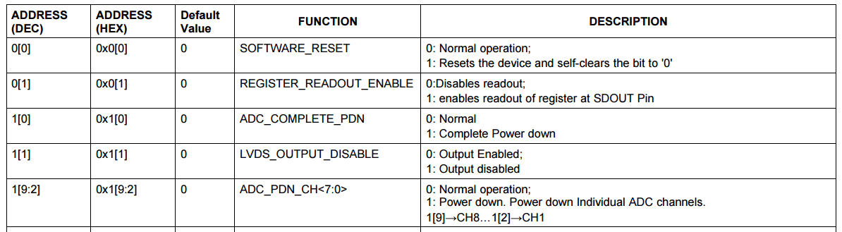
Step 4: Interpret the Register's Bit Fields
This is where you translate functionality into bit values. After the register map, the manual provides a detailed breakdown of each register. For every register, you'll find:
- A diagram showing the bit positions (e.g., 31 down to 0).
- The names of individual bits or multi-bit groups called bit fields.
- A detailed description of what each bit or bit field controls.
Data Sheet Module Structure and Naming Conventions
Let's return to the Microchip document to see how it formally describes register and bit field layouts.
Read the sections 'Modules Description' (focusing on the part about the register description subsection), 'Register Naming Conventions', and 'Bit and Bit Field Naming Conventions'. These sections show exactly how a register is broken down into its functional bit fields, with clear diagrams.
Let's see this in a real-world scenario. Configuring a complex peripheral like SPI requires carefully setting multiple bit fields across several registers.
How To Write An STM32 SPI Driver (Full-Duplex Master Mode)
The video 'How To Write An STM32 SPI Driver' provides a perfect demonstration of this process. The developer needs to configure an SPI peripheral and systematically goes through the control registers, explaining each bit field's purpose by referencing the datasheet.
Watch the segment from 05:30 to 13:12. You don't need to memorize every SPI detail. Instead, focus on the process: how he takes a register (SPI Control Register 1), looks at a bit field (like BR[2:0] for baud rate or CPOL/CPHA for clock mode), explains its function, and decides on the correct value to write.
3. Practical Walkthrough: Configuring a GPIO Pin
Let's consolidate this with a hypothetical example: "Configure pin PC13 as a general-purpose push-pull output."
Your mental workflow should be:
- Goal: Control pin PC13. This pin is part of the
GPIOCperipheral. - Crucial Prerequisite: Enable the Clock. Before a peripheral can be used, its clock must be enabled. This is a very common mistake for beginners. Clock control is usually managed by the Reset and Clock Control (RCC) peripheral.
- Action: Go to the Reference Manual's memory map, find the base address for RCC. Then, go to the RCC chapter, find the appropriate clock enable register for GPIOC (e.g., on STM32, this is the
AHB1ENRregister for GPIOs on the AHB1 bus). Find theGPIOCENbit within that register and set it to 1.
- Action: Go to the Reference Manual's memory map, find the base address for RCC. Then, go to the RCC chapter, find the appropriate clock enable register for GPIOC (e.g., on STM32, this is the
- Find the Peripheral Base Address.
- Action: In the memory map chapter, find the table of peripheral addresses and look up
GPIOC. Let's say it's0x40020800.
- Action: In the memory map chapter, find the table of peripheral addresses and look up
- Configure the Pin Mode. We need to set the pin to "output" mode.
- Action: Go to the GPIO chapter. Find the register map. You'll see a register named
GPIOx_MODER(Mode Register). Let's say its offset is0x00. Its full address is0x40020800 + 0x00.
- Action: Go to the GPIO chapter. Find the register map. You'll see a register named
- Interpret the Bit Fields.
- Action: Look at the detailed description for
GPIOx_MODER. It will show that 2 bits are used to configure each pin. For pin 13, this will be bitsMODER13[1:0], which are bits 27 and 26 of the register. The description table will show:00: Input mode01: General purpose output mode10: Alternate function mode11: Analog mode
- To set pin 13 to output mode, we need to write
01to these bits. This means writing0to bit 27 and1to bit 26.
- Action: Look at the detailed description for
- Configure the Output Type. We want push-pull.
- Action: Back in the GPIO register map, you'll find a
GPIOx_OTYPER(Output Type Register). Let's say its offset is0x04. Its description will show it uses 1 bit per pin. For pin 13, this is bit 13. The table will show:0: Output push-pull (reset state)1: Output open-drain
- We need to ensure bit 13 is
0.
- Action: Back in the GPIO register map, you'll find a
You have now successfully translated the requirement "configure pin PC13 as push-pull output" into a concrete set of register addresses and bit values. The next step, which we'll cover in the next lesson, is to write the C code to perform these modifications safely.
Test your understanding!
You are tasked with writing a UART driver. You look at the UART chapter in the reference manual and find the Status Register (UART_SR). It has a bit named RXNE (Read data register Not Empty) at bit position 5. The description says: "This bit is set by hardware when received data is ready to be read. It is cleared by a read to the Data Register (UART_DR)."
How would you use this information to write a function that safely waits for and reads a single byte?
Show answer
You would implement a polling mechanism.
- Create a
whileloop that continuously reads theUART_SRregister. - Inside the loop, you check if bit 5 (
RXNE) is set to 1. - The loop continues as long as the bit is 0 (
while ((UART_SR & (1 << 5)) == 0)). - Once the loop exits, it means the
RXNEbit is 1, so data is available. - You then perform a read from the
UART_DR(Data Register) to get the received byte. This action also automatically clears theRXNEbit, making the hardware ready for the next reception.
This demonstrates a direct application of interpreting a status bit's functionality from the datasheet to control program flow.
Interview Preparation
-
Question: "You've been handed a new microcontroller you've never seen before and told to write a basic I2C driver. What is your process, and what documents do you start with?"
- Your thought process: Start with the documentation stack. First, get the Reference Manual. I'd navigate to the Memory Map to find the base address for the I2C peripheral I need (e.g.,
I2C1). Then, I'd jump to the I2C chapter. I would immediately look for the Register Map to get a list of all I2C registers and their offsets (CR1,CR2,DR,SR1,SR2, etc.). Before touching any of them, I'd find the RCC (Reset and Clock Control) chapter to figure out which register and bit enables the clock forI2C1. After enabling the clock, I'd go back to the I2C chapter and read the detailed descriptions of the control registers (CR1,CR2) to configure the I2C mode (Master), speed, and addressing. Finally, I'd study the status registers (SR1,SR2) and the data register (DR) to understand the event sequence for a start condition, sending an address, transmitting/receiving data, and generating a stop condition.
- Your thought process: Start with the documentation stack. First, get the Reference Manual. I'd navigate to the Memory Map to find the base address for the I2C peripheral I need (e.g.,
-
Question: "What's the first thing you should do before trying to configure a peripheral's registers?"
- Answer: Enable its clock in the RCC (or equivalent clock management unit). A peripheral without a clock is just a block of inert silicon and its registers will not respond.
Conclusion
You now understand the "art" of navigating hardware documentation. This isn't about memorization; it's about process. By systematically working from the high-level memory map down to individual bit fields, you can confidently interface with any peripheral on any microcontroller.
Key Takeaways:
- Embedded development relies on a documentation stack, with the Reference Manual being the programmer's most critical resource.
- The process for finding register information is: Memory Map -> Peripheral Base Address -> Register Map -> Register Offset -> Bit Field Description.
- Always remember to enable the peripheral's clock before attempting to configure or use it. This is a classic "gotcha".
- Interpreting a datasheet is the skill of translating functional requirements into specific register addresses and the bit values needed to achieve that function.
Next Lesson Preview:
Now that we know which bits to change, the next lesson will focus on the C programming techniques to change them safely. We will master read-modify-write operations using bit masking and bitwise operators to ensure we only affect the bits we intend to, leaving all others in the register untouched.