Hello! Welcome to the next lesson in your interview preparation course.
In our last session, we built an interrupt-driven UART driver and saw why polling was an inefficient method for handling asynchronous data. Today, we're going to flip that script. We will develop a polling-based SPI master driver, and in doing so, explore why polling is often a perfectly valid—and sometimes even preferred—strategy for synchronous communication protocols.
This lesson directly addresses the learning outcome: Develop a polling-based SPI master driver and validate data transfer with a logic analyzer. This is a foundational skill in driver development, and understanding the trade-offs between polling and interrupts for different protocols demonstrates a sophisticated level of embedded systems design knowledge that interviewers look for.
1. SPI Fundamentals and The Case for Polling
Let's start by answering the central question: Why is polling acceptable for SPI when we dismissed it for UART?
The answer lies in the fundamental difference between the protocols:
- UART (Asynchronous): Data can arrive at any time, unexpectedly. If the CPU is busy with another task, it can easily miss an incoming byte. Polling forces the CPU to waste cycles waiting for an event it can't predict.
- SPI (Synchronous): Communication is entirely controlled by the master. No data is ever sent or received unless the master actively generates a clock signal on the SCK line and selects a slave with the Chip Select (CS) pin.
Because the master orchestrates the entire transaction, the data exchange is predictable and sequential. The driver code knows that if it writes a byte to the transmit buffer, a byte will be received from the slave during that same clock cycle. There are no surprise events. In this controlled environment, a simple, blocking polling loop is often the clearest and most straightforward way to implement a transaction.
The main trade-off is that polling is a blocking operation. The CPU is tied up waiting for the hardware flags, unable to do other work. This is fine for quick, atomic operations like configuring a sensor at startup, but it's not suitable for large data transfers that need to happen in the background while the CPU attends to other tasks. For that, you would use an interrupt or DMA-based approach, which we'll cover later.
1.3 Getting Started with SPI - Microchip Online Docs
To refresh our memory on the core concepts of SPI, let's start with this overview from Microchip. It clearly defines the four main signals and the master-slave relationship.
Please read the 'Peripheral Overview' section. Focus on the roles of the four signals: SCK, SDO, SDI, and SS. Pay particular attention to the fact that the master generates the clock and initiates all communication.
2. Implementing a Polling-Based SPI Master Driver
We'll structure our driver into two main parts: an initialization function and data transfer functions. For our examples, we'll refer to the register names common on STM32 microcontrollers, as they are widely used and well-documented. The principles, however, are universal.
Step 1: Driver Initialization
Before any communication can happen, we need to configure the microcontroller's hardware.
Bare-Metal STM32: Setting Up And Using SPI
This article from Hackaday provides a practical guide to setting up an SPI peripheral on an STM32 MCU from scratch. It walks through the necessary register configurations for both the GPIO pins and the SPI module itself.
Please read the section 'Setting Things Up'. It details the sequence of configuration steps. Focus on: Configuring GPIO pins for Alternate Function (AF) mode. Enabling the SPI peripheral clock in the RCC (Reset and Clock Control). Setting the key bits in the SPI Control Registers (SPI_CR1, SPI_CR2), such as baud rate (BR), master mode (MSTR), and data frame format (DFF). Finally, enabling the peripheral with the SPE bit.
Let's synthesize this into a clear initialization sequence. Your SPI_Init() function would perform these steps:
- Enable Clocks: Enable the clock for your chosen SPI peripheral (e.g.,
SPI1) and the GPIO port for its pins (e.g.,GPIOA) in the RCC registers. Without a clock, the peripheral is inactive. - Configure GPIO Pins:
- Set the SCK, MOSI (Master Out Slave In), and MISO (Master In Slave Out) pins to Alternate Function mode. This disconnects them from the general-purpose I/O logic and connects them to the SPI peripheral. You'll need to consult the datasheet to find the correct AF mapping for your specific MCU and pins.
- Set the pin output speed to 'High' or 'Fast' to ensure clean signal edges at high SPI clock rates.
- Configure a separate GPIO pin as a standard push-pull output for the Chip Select (CS) signal. While some MCUs have a hardware
NSSpin, managing it in software with a standard GPIO gives you the flexibility to control multiple slave devices.
- Configure SPI Control Registers (e.g.,
SPI1->CR1andSPI1->CR2):- Set Baud Rate: Choose a clock divider in the
BR[2:0]bits ofSPI_CR1. This divides the peripheral bus clock (e.g., APB2 clock) to generate the final SCK frequency. Always start with a low frequency and increase it once communication is stable. - Set Clock Polarity and Phase: Configure the
CPOLandCPHAbits. These determine the clock's idle state and which clock edge is used to sample data. This must match the slave device's requirement. "Mode 0" (CPOL=0,CPHA=0) is the most common. - Set Master Mode: Set the
MSTRbit to configure the peripheral as the bus master. - Set Frame Format: Set the
DFFbit for 16-bit or 8-bit data frames. Typically 8-bit. Also, ensure you're using MSB-first transmission unless the slave requires otherwise. - Configure Slave Select: Set the
SSM(Software Slave Management) andSSIbits. This tells the SPI hardware that you will control the chip select pin manually using your GPIO output, ignoring the hardwareNSSpin.
- Set Baud Rate: Choose a clock divider in the
- Enable SPI Peripheral: Finally, set the
SPE(SPI Enable) bit inSPI_CR1. The peripheral is now ready for communication.
Step 2: Data Transfer Functions
With the peripheral initialized, we can write functions to send and receive data. The logic relies on polling status flags in the SPI Status Register (SPI_SR).
TXE(Transmit buffer Empty): Set when the transmit buffer is ready to accept a new byte.RXNE(Receive buffer Not Empty): Set when a byte has been fully received and is ready to be read.BSY(Busy): Set while the SPI peripheral is in the middle of a communication.
Here’s a function that performs a full-duplex transfer: it sends a byte and returns the byte that was received simultaneously.
uint8_t SPI_TransmitReceive_Byte(uint8_t data_out) {
    // 1. Wait until the transmit buffer is empty (TXE flag is set).
    // This ensures we don't overwrite data that hasn't been sent yet.
    while (!(SPI1->SR & SPI_SR_TXE)) {
        // This is the polling busy-wait loop.
    }

    // 2. Write the data to the Data Register (DR).
    // This starts the transmission.
    SPI1->DR = data_out;

    // 3. Wait until the receive buffer is not empty (RXNE flag is set).
    // This indicates a byte has been fully received.
    while (!(SPI1->SR & SPI_SR_RXNE)) {
        // Polling loop.
    }

    // 4. Read the received data from the Data Register.
    // Reading DR also clears the RXNE flag.
    return SPI1->DR;
}
To send a block of data, you would wrap this in a loop, bracketed by asserting and de-asserting the chip select line.
void SPI_Transmit_Block(uint8_t* tx_buffer, uint32_t len) {
    // 1. Assert Chip Select (pull the CS pin low)
    CS_LOW();

    // 2. Loop through the data
    for (uint32_t i = 0; i < len; i++) {
        SPI_TransmitReceive_Byte(tx_buffer[i]); // Send data, ignore received byte
    }

    // 3. Wait for the last transmission to complete.
    // This ensures SCK is idle and the slave has processed the last byte.
    while (SPI1->SR & SPI_SR_BSY) {}

    // 4. De-assert Chip Select (pull the CS pin high)
    CS_HIGH();
}
Test your understanding!
To implement a SPI_Receive_Block function that only reads data, what value would you pass to SPI_TransmitReceive_Byte inside its loop, and why?
Show answer
You must send a "dummy" byte for every byte you want to receive. This is because the master must generate a clock signal for the slave to shift its data out. A common dummy value is 0xFF or 0x00. The function call inside the loop would look like rx_buffer[i] = SPI_TransmitReceive_Byte(0xFF);.
A Practical Gotcha: 8-bit vs. 16-bit Register Access
The Hackaday article you read mentioned a subtle but critical bug. On some architectures, the SPI_DR register is physically 16 bits wide. If you write an 8-bit variable to it (SPI1->DR = my_u8_data;), the C compiler might promote the operation to a 16-bit write, sending your byte followed by a garbage byte.
The robust way to ensure an 8-bit write is to cast the register's address to a uint8_t pointer. This forces a byte-wide memory access.
*(__IO uint8_t *)&SPI1->DR = data_out;
This is an excellent detail to bring up in an interview as it demonstrates a deep understanding of how high-level C code interacts with low-level hardware registers.
3. Validating with a Logic Analyzer
Writing a driver is only half the battle; you must prove it works. A logic analyzer or an oscilloscope with protocol decoding is the ultimate tool for this.
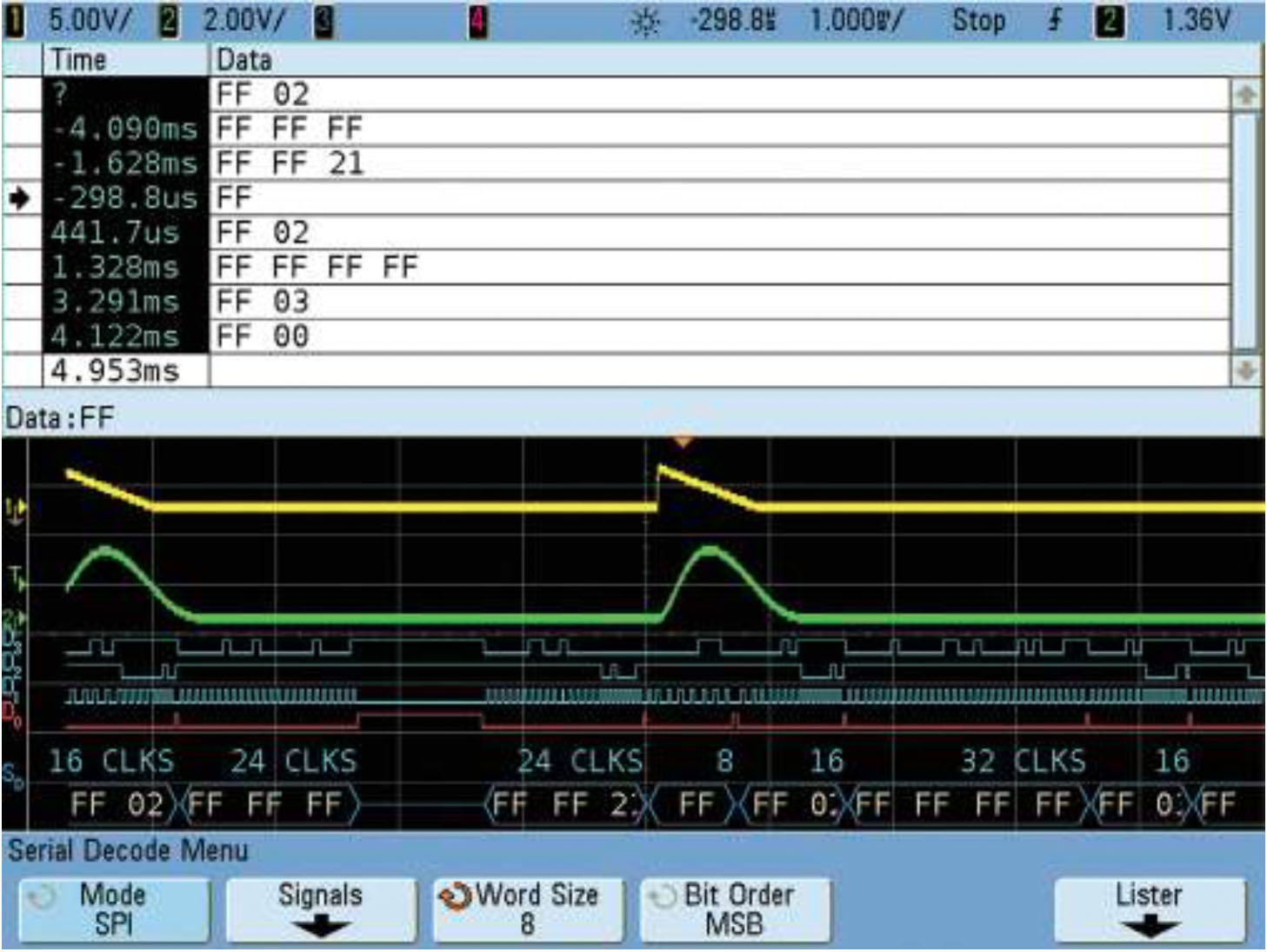
When you connect the probes and capture a transaction, you can verify every aspect of your driver's behavior:
- Chip Select (CS): Does it go low before the clocks start and go high after they finish?
- Clock (SCK): Are the clock pulses present? Is the frequency correct? Is the idle polarity correct (high or low)?
- Data (MOSI/MISO): Is the data changing on the correct clock edge according to your CPHA setting? Is the data decoded by the analyzer matching what you intended to send? Is the slave responding as expected on the MISO line?

Using a logic analyzer transforms debugging from guesswork ("why isn't my sensor responding?") to a deterministic process of observation and correction.
Interview Preparation
Given your experience, an interviewer will want to see that you can not only implement a driver but also reason about its design and debug it effectively.
-
Question: "You've written both interrupt-driven and polling-based drivers. When would you choose a polling-based approach for an SPI driver, and what are its trade-offs?"
- Your Answer: "I'd choose polling for SPI in situations where the data transfers are short, atomic, and part of a sequential process, like initializing a peripheral at startup. The synchronous, master-controlled nature of SPI makes polling a simple and robust choice. The main trade-off is that it's a blocking operation, which ties up the CPU. While simple and easy to debug, it's inefficient for long background transfers, where a DMA or interrupt-based approach would be superior to allow the CPU to perform other tasks."
-
Question: "Describe the register-level polling sequence you would use to send one byte of data over an SPI bus."
- Your Answer: "First, I'd poll the Transmit Empty (
TXE) flag in the status register to ensure the hardware is ready for new data. Once it's set, I'd write the byte to the SPI Data Register (DR). This action initiates the transfer. Then, I would poll the Receive Not Empty (RXNE) flag to know when the transfer is complete and a byte has been received from the slave. Finally, I'd read the Data Register to clear theRXNEflag. To complete the entire transaction, I would poll the Busy (BSY) flag to ensure the peripheral is idle before de-asserting the chip select line."
- Your Answer: "First, I'd poll the Transmit Empty (
-
Question: "You're trying to communicate with a new SPI sensor, but it's not responding. You connect a logic analyzer. What are the first three things you would check on the captured waveform?"
- Your Answer: "First, I'd verify the Chip Select line is being asserted correctly—it must go low for the duration of the transaction. Second, I'd check the SCK signal to confirm the clock is present, its frequency is within the sensor's supported range, and its idle polarity (
CPOL) matches the sensor's datasheet. Third, I'd examine the relationship between the clock edge and the data on the MOSI line to verify my clock phase setting (CPHA) is correct. An incorrect SPI mode is one of the most common integration problems."
- Your Answer: "First, I'd verify the Chip Select line is being asserted correctly—it must go low for the duration of the transaction. Second, I'd check the SCK signal to confirm the clock is present, its frequency is within the sensor's supported range, and its idle polarity (
Conclusion
Today we've built a polling-based SPI master driver, a fundamental component in any embedded developer's toolkit. We've explored not just the how but, more importantly, the why—understanding when and why a simpler, blocking approach is a valid engineering choice.
Key Takeaways:
- Polling is a viable strategy for synchronous, master-controlled protocols like SPI.
- Driver implementation involves GPIO configuration, peripheral clocking, and setting control registers for mode, speed, and data format.
- The core polling loop involves checking the
TXE,RXNE, andBSYstatus flags. - A logic analyzer is an indispensable tool for validating and debugging communication protocols by observing the physical signal behavior.
Next Lesson Preview:
We've covered an asynchronous protocol with interrupts (UART) and a synchronous one with polling (SPI). Next, we'll tackle a protocol that blends these complexities: I2C. In the next lesson, we will develop an interrupt-driven I2C master driver by implementing a state machine. I2C's protocol involves start/stop conditions, addressing, and acknowledgment bits, which makes a state machine an elegant way to manage the transaction's lifecycle, even within an ISR.