Hello! Let's continue our journey into bare-metal driver development.
In our last lesson, we explored the "what" and "why" of GPIO peripherals. We broke down the internal hardware architecture and identified the key configuration registers (MODER, OTYPER, PUPDR, etc.) that define a pin's behavior. You learned the conceptual steps to configure a pin for different roles, like a push-pull output or a pull-up input.
Today, we're moving from theory to practice. Our goal is to implement GPIO driver functions for initializing, reading, and writing digital signals. We'll translate the register-level knowledge from the last lesson into reusable C functions, forming the core of a basic GPIO driver. This is the foundational skill for interacting with any peripheral at the bare-metal level. For you, this is like peeling back the AUTOSAR MCAL layer to see the direct hardware control that happens underneath.
1. From Raw Addresses to Readable Drivers
In bare-metal programming, every peripheral is controlled by writing to specific memory addresses. As we saw, configuring pin PB7 on an STM32 involves addresses like 0x40020400 (GPIOB base) and registers at specific offsets. Writing code full of such "magic numbers" is error-prone and hard to maintain.
A standard and much cleaner approach is to represent peripheral registers as C structs. This allows the C compiler to handle the address offsets for us, leading to more readable and robust code.
Bare-Metal Programming Guide: Human-readable peripherals programming
This guide demonstrates how to transition from cryptic memory addresses to a human-readable programming style using C structs. It's a crucial concept for professional embedded development.
Please read the section 'Human-readable peripherals programming'. Pay close attention to how a GPIO peripheral's registers are mapped to a struct and how this simplifies the code for setting a pin's mode.
As the guide explains, instead of writing:*((volatile uint32_t*)0x40020400) &= ~(3U << 14);*((volatile uint32_t*)0x40020400) |= (1U << 14);
We can write something far more intuitive:GPIOB->MODER &= ~(3U << 14);GPIOB->MODER |= (1U << 14);
This is achieved by defining GPIOB as a pointer to a struct that mirrors the register layout. This is the standard practice you'll find in all vendor-provided header files (like stm32f4xx.h).
2. Implementing the Initialization Function
The most complex part of a GPIO driver is the initialization function. It needs to bring together all the configuration steps we discussed in the last lesson into a single, cohesive operation. A good driver API abstracts these details away from the application developer.
Let's design a function GPIO_Init() that configures a single pin.
Step 1: Clock Enablement
As we learned, no peripheral works until its clock is enabled. Our Init function must handle this first. This is typically done in a separate function, but for simplicity, we'll show it directly. To enable the clock for GPIOB on an STM32F4 series MCU, you'd set bit 1 in the RCC_AHB1ENR register.
RCC->AHB1ENR |= (1 << 1); // Enable clock for GPIOB
Step 2: Configuring Mode, Speed, Type, and Pull
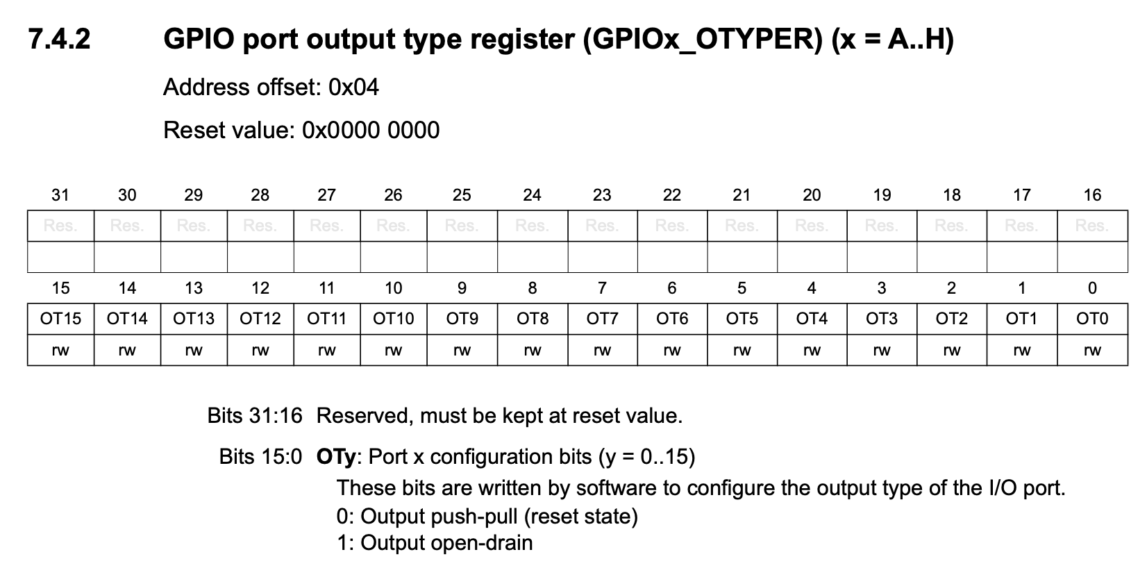
This is where the core configuration happens. We need to perform read-modify-write operations on the MODER, OSPEEDR, OTYPER, and PUPDR registers. Let's focus on the MODER register as an example.
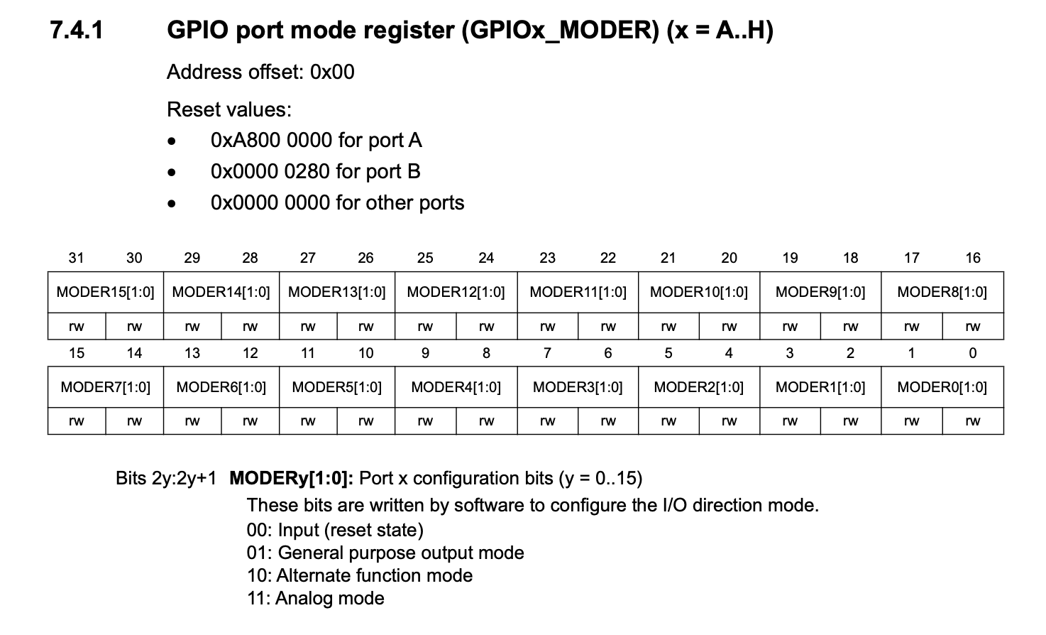
To set pin 7 to output mode (value 01), we must:
- Clear the existing 2 bits for pin 7. These are bits 15 and 14. The mask is
(3U << 14). - Set the new value. The value for output mode is
01. We need to write(1U << 14).
The C code looks like this:
// Assume 'pin' is 7
// 1. Clear the two bits for the target pin
GPIOB->MODER &= ~(3U << (pin * 2));

// 2. Set the desired mode (e.g., 1 for General purpose output)
GPIOB->MODER |= (1U << (pin * 2));
We apply the same read-modify-write logic for the other configuration registers:
OTYPER: 1 bit per pin.OSPEEDR: 2 bits per pin.PUPDR: 2 bits per pin.
3. Implementing Write and Read Functions
Once a pin is initialized as an output or input, we need simple functions to interact with it.
Writing to a Pin: GPIO_WritePin()
You could write to a pin by doing a read-modify-write on the Output Data Register (ODR). However, this is not an atomic operation. If an interrupt occurs between the read and the write, and the ISR also modifies the ODR, one of the changes could be lost.
ARM Cortex-M MCUs provide a better solution: the Bit Set/Reset Register (BSRR).
- Writing a
1to bits0-15ofBSRRsets the correspondingODRbit to 1. - Writing a
1to bits16-31ofBSRRresets the correspondingODRbit to 0. - Writing a
0has no effect.
This allows you to set or reset any bit with a single, atomic write instruction, which is safe to use from both main code and interrupts without needing a critical section.
void GPIO_WritePin(GPIO_TypeDef* GPIOx, uint16_t pin_num, bool state) {
    if (state) {
        // Set the pin high
        GPIOx->BSRR = (1U << pin_num);
    } else {
        // Set the pin low
        GPIOx->BSRR = (1U << (pin_num + 16));
    }
}
Reading from a Pin: GPIO_ReadPin()
Reading is simpler. The state of all pins in a port is available in the Input Data Register (IDR). This is a read-only register. To get the state of a specific pin, you read the whole register and mask out the bit you are interested in.
bool GPIO_ReadPin(GPIO_TypeDef* GPIOx, uint16_t pin_num) {
    if ((GPIOx->IDR & (1U << pin_num)) != 0) {
        return true; // Pin is high
    } else {
        return false; // Pin is low
    }
}
Test your understanding!
A coworker suggests toggling a GPIO pin using GPIOx->ODR ^= (1U << pin_num);. In a system with an RTOS and multiple tasks, what potential issue could this cause that using the BSRR register avoids?
Show answer
The ^= operator expands to a read-modify-write sequence. If a task reads the ODR, and then a context switch occurs before it can write the new value, another task (or an ISR) could modify the ODR in the meantime. When the first task resumes and writes its value, it will overwrite the change made by the other task, leading to a race condition.
The BSRR register is designed to be atomic. A single STR (store) instruction can set or reset a bit without affecting any other bits in the port. This guarantees that the operation completes without interruption, making it safe for concurrent environments.
4. Practical Example: The Blinky
Now, let's put it all together. The following resource provides a step-by-step example of blinking an LED, implementing the very functions we've just designed. It combines clock enablement, pin initialization, and pin writing into a complete application.
STM32 GPIO Registers (Direct Register Access)
This guide provides a full, commented code example for blinking an LED using direct register access. It's a perfect practical demonstration of the driver functions we're building.
Please read the sections 'STM32 GPIO Output (Direct Register Access)' and 'STM32 GPIO Input Read (Direct Register Access)'. Focus on the 'Full Example' code blocks. Notice how they first enable the clock, then configure the registers (CRL in this older STM32F1 family is equivalent to MODER), and finally use BSRR in the main loop.
The resource also introduces the idea of using macros to wrap the BSRR and IDR access. This is a common technique to improve performance over generic HAL functions, as it allows the compiler to inline the register access directly.
#define GPIO_SET_PIN(port, pin)    ((port)->BSRR = (pin))
#define GPIO_CLEAR_PIN(port, pin)  ((port)->BSRR = (pin << 16u))
#define GPIO_READ_PIN(port, pin)   ((port)->IDR & (pin))
These macros are extremely fast, often compiling down to a single instruction.
Interview Preparation
-
Question: "Walk me through how you would write a C function to initialize a GPIO pin as a push-pull output. What registers are involved and in what order?"
- Your Answer: "First, the function would need to enable the clock for the corresponding GPIO port in the RCC peripheral's clock enable register, for example,
RCC_AHB1ENR. Without the clock, the peripheral is inactive. Second, I would configure the pin's mode by writing01to the appropriate 2-bit field in theGPIOx_MODERregister. Third, I'd set the output type to push-pull by writing0to the corresponding bit in theGPIOx_OTYPERregister. Finally, I would configure a suitable slew rate in theGPIOx_OSPEEDRand ensure no pull-up/pull-down is active in theGPIOx_PUPDR. All configuration steps would use atomic read-modify-write operations to avoid affecting other pins on the same port."
- Your Answer: "First, the function would need to enable the clock for the corresponding GPIO port in the RCC peripheral's clock enable register, for example,
-
Question: "You need to write a GPIO pin's state from both the main application loop and an Interrupt Service Routine. Why is it preferable to use the
BSRRregister instead of modifying theODR?"- Your Answer: "Modifying the
ODRrequires a read-modify-write sequence, which is not atomic. If the main loop reads theODRand is then preempted by the ISR which also modifies theODR, a race condition can occur, and one of the changes will be lost when the main loop resumes and writes its old value. TheBSRRsolves this by providing an atomic, one-shot mechanism. A single write toBSRRcan set or reset a specific pin without affecting any other pins, guaranteeing data integrity in a concurrent environment without needing to disable interrupts."
- Your Answer: "Modifying the
-
Question: "When writing a bare-metal driver, how do you handle peripheral register addresses to make the code readable and portable?"
- Your Answer: "Instead of hardcoding memory addresses, which are 'magic numbers', the standard practice is to define a
structthat maps to the peripheral's register layout. Then, you define a pointer to this struct type, initialized to the peripheral's base address. For example,#define GPIOB ((GPIO_TypeDef *) 0x40020400). This allows you to access registers with clear, readable syntax likeGPIOB->MODERinstead of pointer arithmetic. This approach is used by all MCU vendors in their device header files, making the code more portable and maintainable."
- Your Answer: "Instead of hardcoding memory addresses, which are 'magic numbers', the standard practice is to define a
Conclusion
In this lesson, we bridged the gap between theory and implementation. You've learned how to translate datasheet register descriptions into a functional, reusable set of C functions that form the basis of a hardware driver.
Key Takeaways:
- Abstraction is Key: Good driver design involves creating functions (
Init,Write,Read) that hide the low-level register complexity. - Readable Code: Use
structsto map peripheral registers, avoiding raw memory addresses. - Safe Configuration: Master atomic read-modify-write operations (clear-then-set) to configure registers without side effects.
- Efficient I/O: Use specialized registers like
BSRRfor atomic and efficient pin manipulation, a critical practice in real-time and multi-threaded systems.
Next Lesson Preview:
In this lesson, and the last, we've seen that the very first step to using any peripheral is enabling its clock. But where do these clocks come from? How are they generated and controlled? In the next lesson, we will dive into this critical topic and explain the architecture of a microcontroller clock tree, including oscillators, PLLs, and prescalers.